Spatial light modulator and mirror device

a technology of spatial light and mirror device, which is applied in the field of spatial light modulator implementation of display apparatus, can solve the problems of affecting the quality of images, limiting the use of high-quality images, and limiting the quality of display, so as to improve the miniaturization and performance characteristics manufactured with a low production cost, reduce cost, and impact siz

Inactive Publication Date: 2011-06-28
SILICON QUEST KABUSHIKI KAISHA +1
View PDF30 Cites 2 Cited by
  • Summary
  • Abstract
  • Description
  • Claims
  • Application Information

AI Technical Summary

Benefits of technology

[0016]Therefore, one aspect of the present invention is to provide a spatial light modulator and a mirror device to achieve improved miniaturization and performance characteristics manufactured with a low production cost. A display system with spatial light modulator can therefore be provided with a reduce cost, impact size and high performance characteristics.
[0017]The present invention discloses a spatial light modulator includes a plurality of pixel elements disposed on a substrate. Each of the pixel elements comprises a deflectable micromirror. Specifically, instead of SRAM, the spatial light modulator is implemented with a DRAM in each of the pixel elements. The DRAM in each of the pixel elements has a smaller number of transistors than SRAM. The spatial light modulator can be manufactured with smaller pixel size and circuit configuration with improved withstand voltage. Further improvements can also be achieved for manufactured the spatial light modulator with smaller capacitor with better layout configuration for wire connections and control signal transmissions.

Problems solved by technology

Even though there have been significant advances made in recent years in the technologies of implementing electromechanical micromirror devices as spatial light modulators (SLM), there are still limitations and difficulties when they are employed to display high quality images.
Specifically, when the display images are digitally controlled, the quality of the images is adversely affected because the images are not displayed with a sufficient number of gray scale gradations.
The on-and-off states of the micromirror control scheme as that implemented in the U.S. Pat. No. 5,214,420, and in most conventional display systems, impose a limitation on the quality of the display.
Due to the ON-OFF states implemented in the conventional systems, there is no way of providing a shorter pulse width than the duration represented by the LSB.
The limited levels of the gray scale lead to a degradation of the display image.
However, in these conventional techniques, if each pixel is equipped with Static Random Access Memory (SRAM) and if an ON / OFF control for the pixel is performed together with the bias-driving of the micromirror, there will be a technical problem in that one piece of SRAM requires at least five transistors, which need to be accommodated in the region of the pixel.
Consequently, the size of the pixel cannot be reduced, resulting in increasing the size of a silicon substrate (i.e., a chip size) with an increase in the number of required pixels.
This in turn increases the cost of a display device while making it difficult to reduce the size of a display apparatus.
However, this technique increases the number of masks in the photolithography process and thus complicates the production process and increases the cost of the display device.
Furthermore, for a high definition and high density pixel configuration, wirings used for controlling transistors cannot be made thick enough, and consequently, the drive speed of the transistors, that is, the micromirror, is reduced due to stray capacitance and wiring resistance.
Thus the performance of the display device is not improved.

Method used


Image

  • Spatial light modulator and mirror device
  • Spatial light modulator and mirror device
  • Spatial light modulator and mirror device

Examples


Embodiment Construction

[0076]The following is a description, in detail, of the preferred embodiment of the present invention with reference to the accompanying drawings.

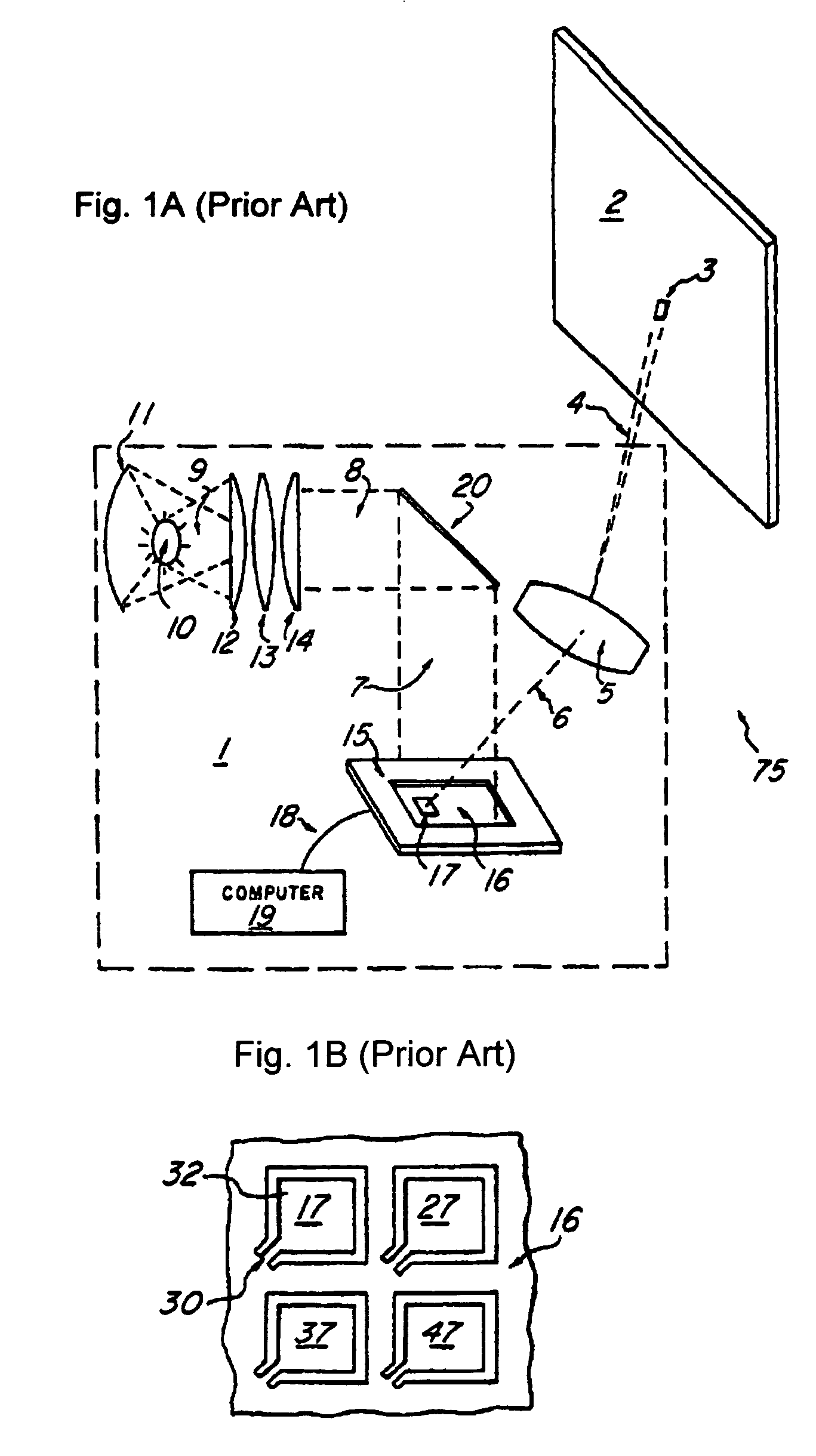
[0077]FIG. 2 is a top view diagram showing a diagonal perspective view of a mirror device according to a preferred embodiment of the present invention in which the mirror device is incorporated in a projection system as a spatial light modulator.

[0078]The projection apparatus 100 including a spatial light modulator 200 according to the present embodiment comprises a control apparatus 300, light source 510 and projection optical system 520.

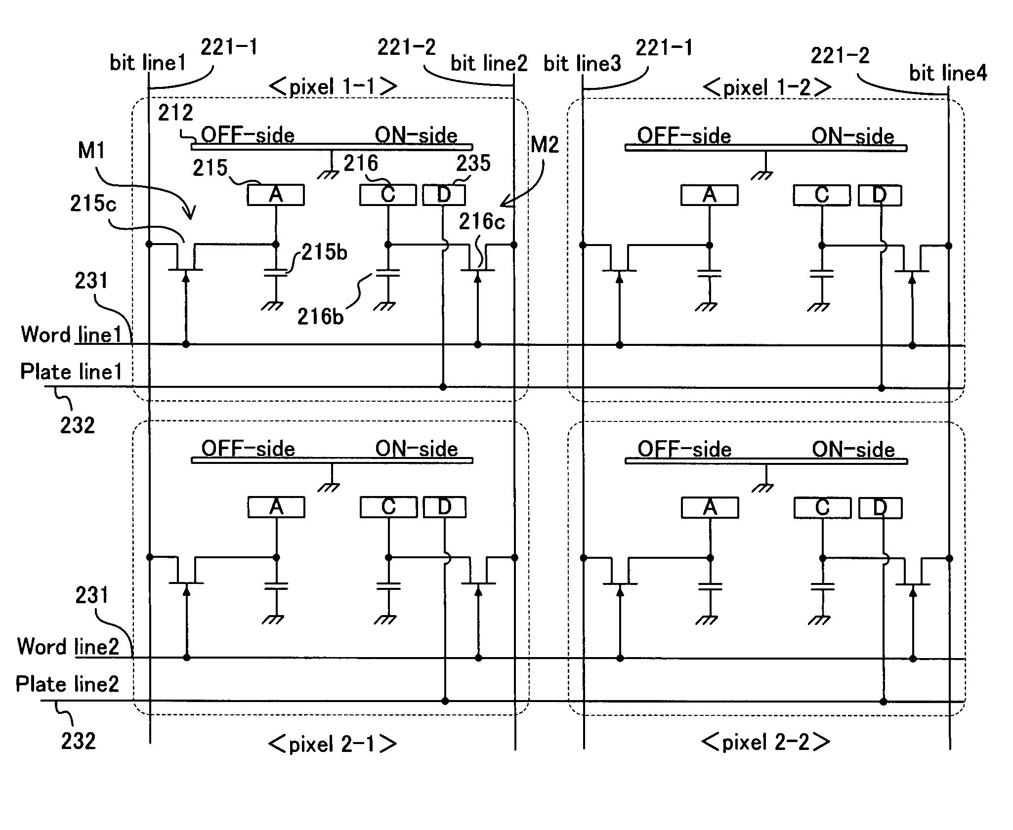
[0079]As shown in FIG. 2, the spatial light modulator 200 is configured to arrange, cross-wise in two dimensions on a substrate 214, a plurality of pixel units 211, each of which is constituted by an address electrode (not shown), an elastic hinge (not shown) and a mirror supported by the elastic hinge. In the configuration shown in FIG. 2, the pixel units 211 each comprising a square mirror 212 are arran...


PUM


Abstract

The present invention discloses a spatial light modulator includes a plurality of pixel elements disposed on a substrate. Each of the pixel elements comprises a deflectable micromirror. Specifically, instead of SRAM, the spatial light modulator is implemented with a DRAM in each of the pixel elements. The DRAM in each of the pixel elements has a smaller number of transistors than SRAM. The spatial light modulator can be manufactured with smaller pixel size and circuit configuration with improved withstand voltage. Further improvements can also be achieved for manufactured the spatial light modulator with smaller capacitor with better layout configuration for wire connections and control signal transmissions.

Description

CROSS REFERENCE TO RELATED APPLICATIONS[0001]This application is a Non-provisional application of a Provisional application 61 / 133,718 filed on Jul. 1, 2008 and a Continuation in Part (CIP) application of a patent application Ser. No. 12 / 072,448 filed on Feb. 25, 2008 now U.S. Pat. No. 7,839,561. The Non-provisional application Ser. No. 12 / 072,448 is a Continuation in Part (CIP) application of U.S. patent application Ser. No. 11 / 121,543 filed on May 4, 2005, now issued into U.S. Pat. No. 7,268,932. The application Ser. Nos. 12 / 072,448 and 11 / 121,543 are further Continuation in part (CIP) applications of three previously filed applications. These three applications are Ser. Nos. 10 / 698,620 now abandoned; 10 / 699,140, now issued into U.S. Pat. No. 6,862,127; and Ser. No. 10 / 699,143, now issued into U.S. Pat. No. 6,903,860. All three patents were filed on Nov. 1, 2003 by one of the applicants of this patent application. The disclosures made in these patent applications are hereby incorp...

Claims


Application Information

Patent Timeline
Patent Type & Authority Patents(United States)
IPC IPC(8): G09G3/34G09G3/20G02B26/00
CPCG02B26/0841G09G3/346G09G3/2014G09G3/2022G09G2300/0857G09G2300/0426G09G2300/0439G09G2300/0842
Inventor SUGIMOTO, NAOYAMAEDA, YOSHIHIROISHII, FUSAO
Owner SILICON QUEST KABUSHIKI KAISHA
Why Eureka
Try Eureka