Pixel driving circuit and driving method thereof

A pixel driving circuit and driving method technology, applied in static indicators, instruments, etc., can solve problems such as inability to accurately eliminate display unevenness, achieve improved ability to suppress uneven voltage distribution, high practical value, and increase aperture ratio Effect

Active Publication Date: 2013-02-06
BOE TECH GRP CO LTD
View PDF5 Cites 36 Cited by
  • Summary
  • Abstract
  • Description
  • Claims
  • Application Information

AI Technical Summary

Problems solved by technology

[0004] However, in the prior art, the design of most AMOLED pixel driving circuits can only compensate the threshold voltage of the driving tube to a certain extent, and cannot accurately eliminate the problem of uneven display caused by uneven threshold distribution.

Method used


Image

  • Pixel driving circuit and driving method thereof
  • Pixel driving circuit and driving method thereof
  • Pixel driving circuit and driving method thereof

Examples


Embodiment 1

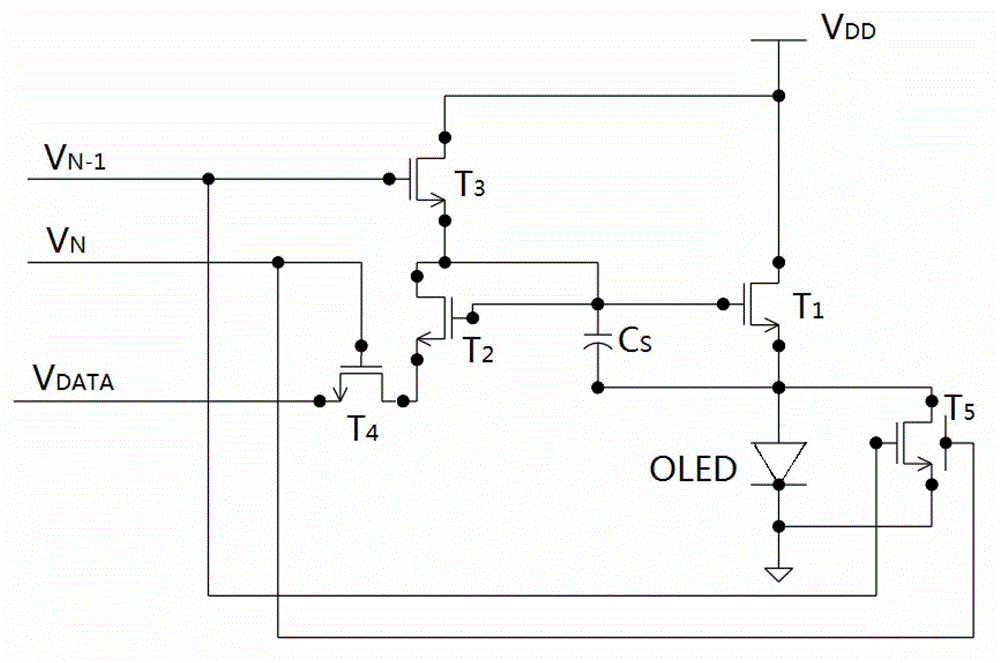
[0037] The pixel driving circuit of the present invention includes: a first transistor T1 to a fourth transistor T4, a storage capacitor C S , organic light-emitting diode OLED, bypass circuit, data line, N-1th scanning line V N-1 and the Nth scan line V N ;in,

[0038] The drain of the first transistor T1 is connected to the power supply voltage, and the gate is connected to the storage capacitor C S The first end of the source is connected to the storage capacitor C S The second terminal of the OLED and the anode of the OLED;

[0039] The drain and gate of the second transistor T2 are connected to the storage capacitor C S The first end of the first terminal, the source of the third transistor T3 and the gate of the first transistor T1, the source is connected to the drain of the fourth transistor T4;

[0040] The gate of the third transistor T3 is connected to the N-1th scanning line, the drain is connected to the power supply voltage, and the source is connected to th...

Embodiment 2

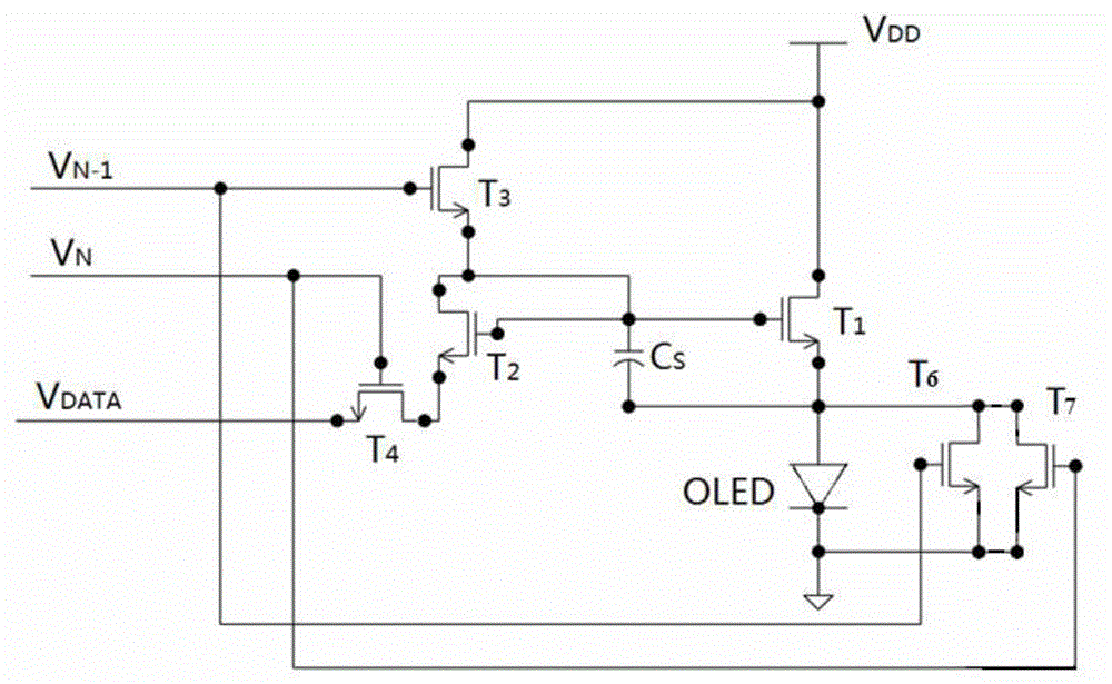
[0055] In this embodiment, the bypass circuit is the sixth transistor and the seventh transistor T6 and T7 connected in parallel with the OLED, the drains of T6 and T7 are respectively connected to the anode of the OLED, the sources of T6 and T7 are grounded, and the gate of T6 Pole connected to the N-1th scan line V N-1 , the gate of T7 is connected to the Nth scan line V N , other circuit connections are the same as those in Embodiment 1, such as figure 2 shown.

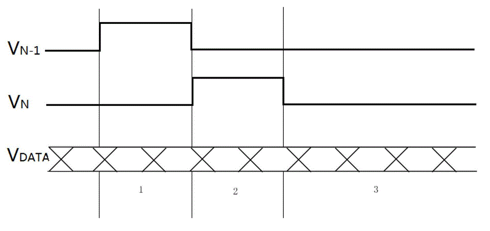
[0056] The driving scheme of the above-mentioned pixel driving circuit includes the following steps:

[0057] 1) Preset stage: N-1th scan line V N-1 is high and the Nth scan line V N is low level, at this stage, the second transistor T2, the third transistor T3 and the sixth and seventh transistors T6 and T7 are turned on, and the power supply voltage V DD on the storage capacitor C S precharged to supply voltage V DD ;

[0058] 2) Adjustment stage: N-1th scan line V N-1 is low and the Nth scan line V N ...


PUM


Abstract

The invention discloses a pixel driving circuit and a driving method thereof. The pixel driving circuit comprises a first transistor, a second transistor, a third transistor and a fourth transistor, storage capacitors, an organic light emitting diode (OLED), a bypass circuit, a data line, an N-1st scanning line and an Nth scanning line. A second end of the storage capacitor is connected with a source electrode of the first transistor, and the OLED is connected with the bypass circuit in parallel, so that current flowing through the OLED is completely determined by data voltage and is irrelevant to threshold voltage of the first transistor; the current flowing through the OLED completely relays on the data voltage of the data line, without increasing the number of the transistors, the capacitors and control lines too much, the threshold voltage can be accurately compensated in order to maintain uniformity and constancy of the display brightness, the aperture ratio and the display resolution can be improved easily, and the capability of inhibiting nonuniform distribution of the threshold voltage is improved; therefore, the pixel driving circuit and the driving method thereof have a relatively high practical value and can be expected to be widely used in a microelectronic industry and a flat panel display industry.

Description

technical field [0001] The invention belongs to the field of flat panel display, and in particular relates to a pixel driving circuit and a driving method thereof. Background technique [0002] Active Matrix Organic Light-Emitting Diode (Active Matrix Organic Light-Emitting Diode) AMOLED has the advantages of small size, simple structure, self-illumination, high brightness, good picture quality, large viewing angle, low power consumption and short response time, etc. Therefore, it has attracted widespread attention and is likely to become a next-generation display technology to replace liquid crystals. [0003] Currently, TFTs used to drive AMOLEDs mainly include amorphous silicon thin film transistors and polysilicon thin film transistors. Due to the current-driven characteristics of organic light-emitting diodes (OLEDs), OLEDs require a large current to drive, because amorphous silicon thin film transistors cannot provide sufficient driving current due to low carrier mobi...

Claims


Application Information

Patent Timeline
Patent Type & Authority Applications(China)
IPC IPC(8): G09G3/32G09G3/3258
Inventor 韩德栋蔡剑王龙彦刘盖王亮亮马建忠丛瑛瑛张翼田宇张索明单东方黄福青王漪张盛东刘晓彦康晋锋
Owner BOE TECH GRP CO LTD
Why Eureka
Try Eureka