Method for manufacturing copper PCB (Printed Circuit Board) circuit

A technology for making PCB boards and circuits. It is used in the manufacture of printed circuits, removal of conductive materials by chemical/electrolytic methods, and printed circuits. It can solve problems such as cracked substrates, ink accumulation on both sides of the circuit, and threats to the reliability of PCB boards.

Active Publication Date: 2013-02-06
JIANGNAN INST OF COMPUTING TECH
View PDF2 Cites 23 Cited by
  • Summary
  • Abstract
  • Description
  • Claims
  • Application Information

AI Technical Summary

Problems solved by technology

[0004] Moreover, for thick copper printed boards, there is a large drop between the copper surface and the base material. It is difficult to apply oil between the lines during screen printing solder mask, and multiple scrapes are required. Because the copper on the board is thicker, the conductor The accumulation of ink on both sides of the line is much higher than the thickness of the ink on the substrate, so that some air in the ink is ambushed and cannot be drained away during the pre-baking heating solvent volatilization process, because the ink is thicker and the solvent volatilizes to form solder resist Bubbles 3 and pinholes
[0005] Moreover, the thermal expansion coefficient of ink 4 is relatively large, and the thicker the solder resist ink between conductor lines, the more serious problems such a

Method used


Image

  • Method for manufacturing copper PCB (Printed Circuit Board) circuit
  • Method for manufacturing copper PCB (Printed Circuit Board) circuit
  • Method for manufacturing copper PCB (Printed Circuit Board) circuit

Examples


Embodiment Construction

[0028] In order to make the content of the present invention clearer and easier to understand, the content of the present invention will be described in detail below in conjunction with specific embodiments and accompanying drawings.

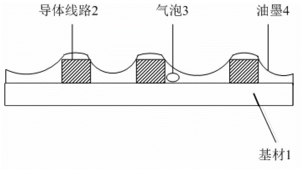
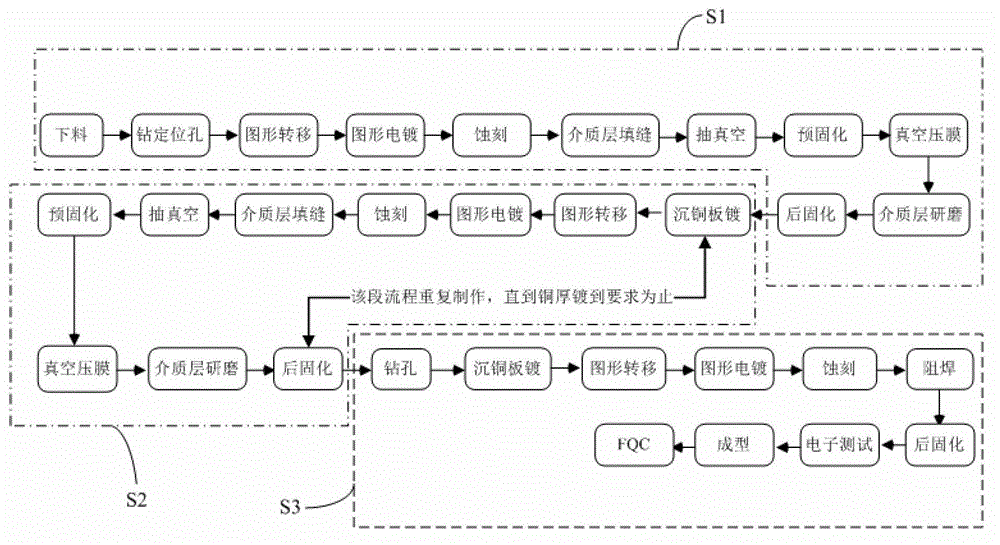
[0029] The present invention fills the medium layer ink with similar or the same expansion coefficient (CTE) as the epoxy plate between the lines by screen printing layer by layer, ensuring that there is no air in the filled ink and that it is very tightly combined with the substrate and the line wall, so as to achieve reduction The purpose of the drop between the base material and the copper surface. In addition, solder resist printing can be performed when the remaining copper thickness is normal (for example, when the predetermined copper thickness is reached).

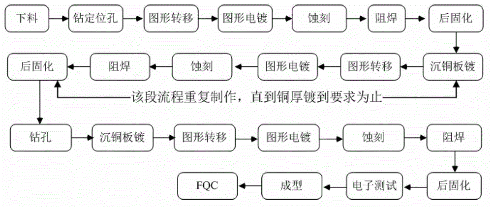
[0030] Specifically, image 3 It schematically shows the flow of the method for fabricating thick copper PCB board circuit according to the embodiment of the present invention. The...


PUM


Abstract

The invention provides a method for manufacturing a thick copper PCB (Printed Circuit Board) circuit. The method comprises the steps of: a positioning hole drilling step for drilling a positioning hole in a printed board substrate; a pattern transfer step for bonding a dry film on the printed board substrate and forming patterns on the dry film; a pattern electroplating step for electroplating copper on the patterns unprotected by the dry film; a film removing step to remove the dry film; an etching step for etching the copper unprotected by lead and tin and removing the lead and tin to obtain a conductor circuit pattern of a current layer; a dielectric layer joint filling step for arranging a dielectric layer oil ink layer on all the substrate area of a circuit board; a dielectric layer grinding step for removing oil ink on a copper face; a post-curing step for curing the structure; a copper deposition electroplating step for depositing a copper deposited metal layer on a circuit copper layer and the surface filled with the dielectric layer oil ink; and a full-board electroplating step for electroplating copper on the entire circuit board. When the final thickness of copper does not reach the preset thickness of the copper, the steps from pattern transfer to full-board electroplating are executed repeatedly.

Description

technical field [0001] The invention relates to the field of semiconductor manufacturing, and more specifically, the invention relates to a method for manufacturing thick copper PCB circuit boards. Background technique [0002] The copper thickness requirements of the commonly used circuit boards are mainly in the range of 18-200μm. With the continuous development of electronic technology, electronic products have higher and higher requirements for the current carrying capacity and self-heating performance of PCBs. Therefore, the copper thickness of circuit boards is required to be to thicker. However, it is difficult to etch the circuit and make the solder resist on the PCB board with copper thickness > 200 μm. The existing technology for manufacturing thick copper board is the layer-by-layer stacking circuit method. The method is to use multiple platings, and after each plating etch, the substrate (such as figure 2 1) is filled with solder resist ink and post-cured, t...

Claims


Application Information

Patent Timeline
IPC IPC(8): H05K3/00H05K3/06
Inventor 牟冬吴小龙吴梅珠徐杰栋刘秋华胡广群梁少文
Owner JIANGNAN INST OF COMPUTING TECH
Why Eureka
Try Eureka