Supercharge Your Innovation With Domain-Expert AI Agents!

Method of producing circuit board by additive method, and circuit board and multilayer circuit board obtained by the method

一种多层电路板、电路板的技术,应用在多层电路制造、三维刚性印刷电路板、电路等方向,能够解决制造过程复杂、导电率烦恼、线路强度恶化等问题

Inactive Publication Date: 2013-02-06
PANASONIC CORP
View PDF11 Cites 0 Cited by
  • Summary
  • Abstract
  • Description
  • Claims
  • Application Information

AI Technical Summary

Problems solved by technology

However, this method requires preparing two photosensitive resin layers with different solvent solubility, developing them with two solvents, and dissolving the second photosensitive resin with an alkaline solution after adsorbing the catalyst, so the manufacturing process is very complicated.
[0019] Preparing circuits with narrow line widths and line spacings by using the circuit forming method as described above also causes the following problems: Specifically, reducing the line widths and line spacings of the circuits leads to deterioration of line strength
[0024] Resin smear 305 remaining on bottom of IVH 304 may cause conductivity annoyance

Method used


Image

  • Method of producing circuit board by additive method, and circuit board and multilayer circuit board obtained by the method
  • Method of producing circuit board by additive method, and circuit board and multilayer circuit board obtained by the method
  • Method of producing circuit board by additive method, and circuit board and multilayer circuit board obtained by the method

Examples


no. 1 example

[0054] First Embodiment (Method of Manufacturing Circuit Board by Using Expandable Resin Film)

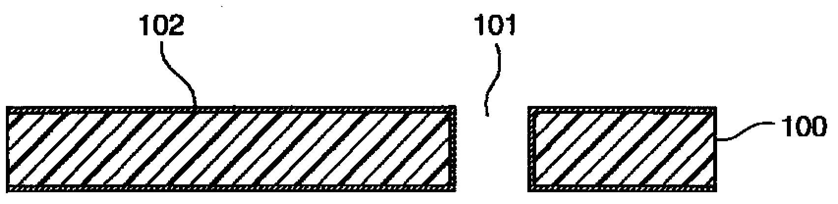
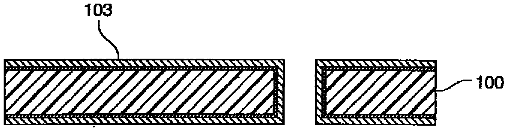
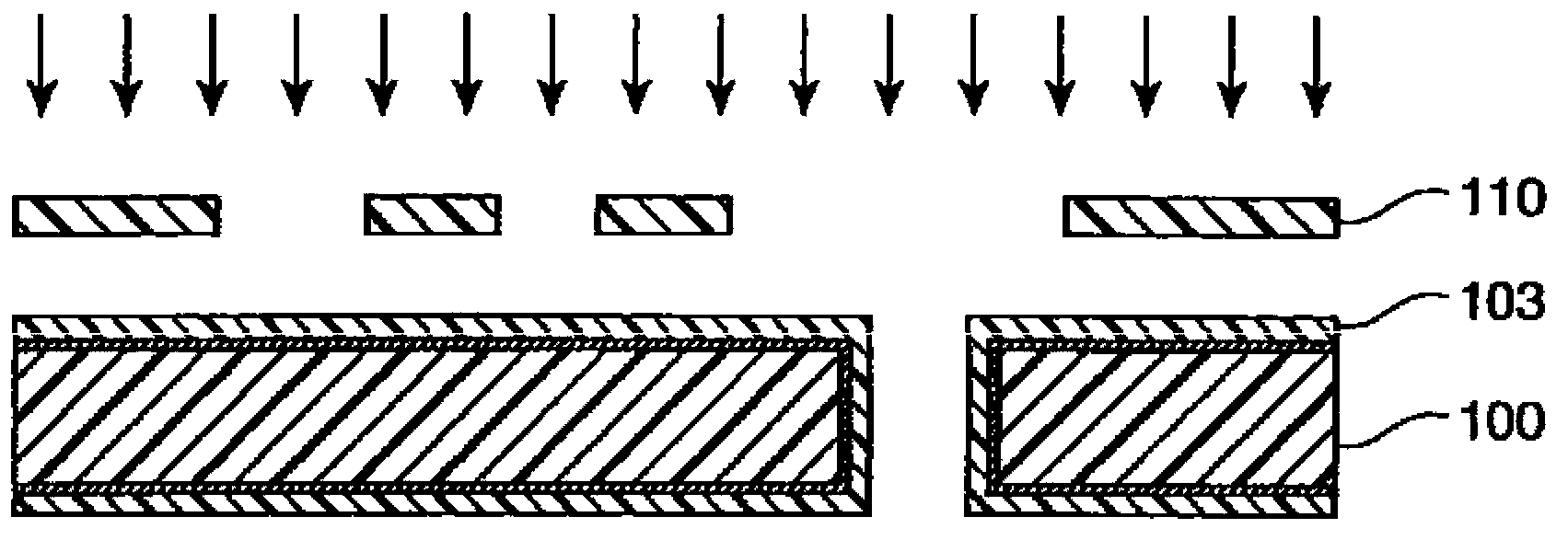
[0055] A method of manufacturing a circuit board in this embodiment will be described with reference to the drawings. Figures 5A to 5E is a schematic cross-sectional view illustrating the steps of the method of manufacturing a circuit board in the first embodiment. exist Figures 5A to 5E 2, an expandable resin film; 3, a circuit groove; 4, a through hole passing through a part of the circuit groove 3; 5, a plating catalyst; and 6, an electroless plating film. In the manufacturing method of this embodiment, as Figure 5A As shown, an expandable resin film 2 is first formed on the surface of an insulating substrate 1 . The expandable resin film means a resin film that is easily separated from the substrate surface by swelling with a special liquid.

[0056] Various organic substrates used in manufacturing circuit boards can be used as the insulating substrate 1 without particul...

example 1

[0095] A styrene-butadiene copolymer (SBR) film having a thickness of 2 μm was formed on the surface of an epoxy resin substrate (R1766 manufactured by Matsushita Electric Works Co., Ltd.) having a thickness of 100 μm. By coating a suspension of styrene-butadiene copolymer (SBR) in methyl ethyl ketone (MEK) (manufactured by Zeon Corporation, acid equivalent: 600, particle diameter: 200 nm, solid matter: 15%) It was spread on the principal surface of the epoxy resin substrate, and the resulting coating film was dried at 80° C. for 30 minutes to form a film.

[0096] A groove having an approximately rectangular cross-section with a width of 20 μm and a depth of 30 μm was formed on the film-formed epoxy resin substrate through laser processing. A model 5330 manufactured by ESI equipped with a UV-YAG laser was used for this laser processing.

[0097] The laser-processed epoxy substrate was then dipped in a detergent conditioner (surfactant solution pH<1, C / N 3320, manufactured by...

no. 2 example

[0105] Second Embodiment (Method of Forming Local Reinforcement Structure in Fine Wiring)

[0106] By carrying out the method of manufacturing a circuit board described in the first embodiment, it is possible to form a local reinforcement structure to be described below for local reinforcement of circuits.

[0107] The method of manufacturing a circuit board in this embodiment will be described specifically with reference to the drawings. To prevent repetition, only those common to those in the description of the first embodiment will be briefly described.

[0108] Figures 7A to 7E are schematic cross-sectional views respectively explaining the steps of the method of manufacturing a circuit board in the second embodiment.

[0109] In the manufacturing method of this embodiment, as Figure 7A As shown, the resin film 12 is first formed on the surface of the insulating substrate 1 .

[0110] Various organic substrates similar to those described in the first embodiment can b...


PUM


Abstract

The method of producing a circuit board includes a film-forming step of forming a resin film on the surface of an insulative substrate, a circuit groove-forming step of forming circuit grooves having a depth equal to or greater than the thickness of the resin film on the external surface of the resin film, a catalyst-depositing step of depositing a plating catalyst on the surface of the circuit grooves and the surface of the resin film, a film-separating step of separating the resin film, and a plating processing step of forming an electrolessly plated film after separation of the resin film, wherein in the circuit groove-forming step, a regional reinforced structure is formed in circuit groove regions. The present invention also provides a circuit board and a multilayer circuit board obtained by the method.

Description

[0001] This application is a divisional application of the following application: [0002] Filing date of the original application: April 30, 2009 [0003] The application number of the original application: 200980111817.3 [0004] Title of invention of the original application: Method for manufacturing circuit boards by additive method, circuit boards and multilayer circuit boards obtained by this method technical field [0005] The invention relates to a method for manufacturing circuit boards by an additive process, as well as circuit boards and multilayer circuit boards obtained by the method. Background technique [0006] Recently, there has been a rapid increase in the functionality of electrical equipment including portable information systems such as mobile phones, computers and their peripherals, various information home appliances, and the like. Accompanied by this trend, there has been an increased need to increase circuit density on circuit boards used in these...

Claims


Application Information

Patent Timeline
Patent Type & Authority Applications(China)
IPC IPC(8): H05K3/10H05K3/18H05K3/46H05K1/02
CPCH05K2203/0565H05K1/111H05K3/465H05K2201/09845H05K3/4647H05K1/0206H05K1/0284H01L2224/48227H05K2201/09736H05K2203/0108H05K1/162H05K3/0032H01L2924/15311H05K1/0269H05K3/184H05K3/4661H05K3/107H05K2203/161H05K2201/2072H05K1/02H05K3/10H05K3/18H05K3/46
Inventor 吉冈慎悟藤原弘明
Owner PANASONIC CORP
Features
  • R&D
  • Intellectual Property
  • Life Sciences
  • Materials
  • Tech Scout
  • Unparalleled Data Quality
  • Higher Quality Content
  • 60% Fewer Hallucinations
Learn More