Seamless optical splicing method for 3*3 flat detectors

An area array detector, optical splicing technology, applied in optics, optical components, instruments, etc., can solve the problems of many times of light splitting, the relative relationship between prisms is independent and not concentrated, and the position is asymmetric, so as to achieve small volume and light weight structure, prism Strong and reliable, the effect of ensuring stability

Inactive Publication Date: 2014-11-26
INST OF OPTICS & ELECTRONICS - CHINESE ACAD OF SCI
View PDF5 Cites 4 Cited by
  • Summary
  • Abstract
  • Description
  • Claims
  • Application Information

AI Technical Summary

Problems solved by technology

[0005] Chen Xunan et al. In the focal plane optical splicing technology of multi-slice area CCD image sensor, the single-lens optical splicing method can realize the splicing of multi-slice area CCD, but the number of light splitting is too many, the loss of light energy is serious, and the working distance behind the optical system is required to be large. However, it cannot be realized in the large field of view surveying and mapping camera system or there is a serious shortage of light energy
[0006] Chinese invention patent CN 101650423 B’s optical splicing of large area array photoelectric devices can only realize the splicing of area array detectors in 2×3 or 2×2 modes, the positions of the prisms used for light splitting are asymmetrical, and the structure and splicing of the prisms are complicated; The contact surface is small and it is difficult to guarantee long-term working stability; the relative relationship between each prism is independent and not centralized, and splicing requires complex mechanical structures for fixing and installation, which is large in size and heavy in weight, which does not meet the needs of lightweight aerospace

Method used


Image

  • Seamless optical splicing method for 3*3 flat detectors
  • Seamless optical splicing method for 3*3 flat detectors

Examples


Embodiment Construction

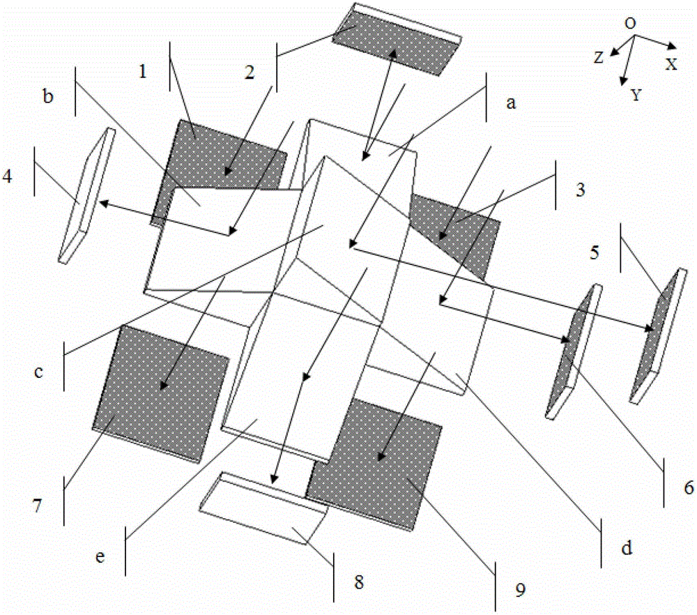
[0029] like figure 1 As shown, the present invention includes 5 reflecting prisms and 9 area array detectors, such as 10k×10k area array detectors.

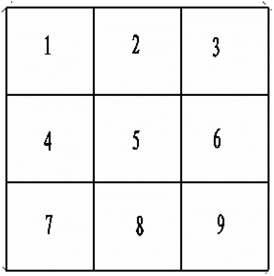
[0030] like figure 2 As shown, the combined image plane arrays are numbered from top to bottom and from left to right, that is, the top row is the first row, the bottom row is the third row; the leftmost column is the first column, and the rightmost column is the third row. List. The first row is area array detectors 1~3, the second row is area array detectors 4~6, and the third row is area array detectors 7~9; the combined image plane is divided according to the array and the 9 area array detectors are respectively combined correspondingly Areas 1 to 9 on the image plane.

[0031] Establish a space rectangular coordinate system, the origin O is located in the upper left corner of the image plane; the X axis is the column increasing direction, that is, from left to right; the Y axis is the row increasing direction, that is, f...


PUM


Abstract

The invention discloses a seamless optical splicing method for 3*3 flat detectors. A symmetric prism structure is adopted for image plane light splitting, four flat detectors are arranged on an optical axis perpendicular transmission image plane, and five flat detectors are arranged on four side faces. A few of spliced structures are symmetric, simple and distributed in a centralized way, and energy is not lost after total-reflection total-transmission light splitting. The seamless splicing method can be applied to aviation and aerospace optical imaging, optical detection instruments and equipment and is particularly suitable for aviation and aerospace imaging photoelectric systems of extra-large flat detectors.

Description

technical field [0001] The invention belongs to a seamless optical splicing method for a super large area array detector, in particular to a seamless optical splicing method for realizing a 3×3 area array detector by adopting a symmetrical prism structure. Background technique [0002] With the development of aviation and aerospace technology, the demand for photoelectric imaging systems of large area arrays and super large area arrays is becoming more and more urgent. Two methods are often used to achieve large-scale area array imaging. One is to customize ultra-large area array detector devices in the area array detector manufacturer, and the other is to use area array detectors for splicing. [0003] At present, the size of the single-chip large area array detector in the world is about 17k×15k (DMC250), which is not a shelf commodity and the application cost is expensive. In addition, further increasing the scale of the monolithic area array detector is also a technical...

Claims


Application Information

Patent Timeline
Patent Type & Authority Patents(China)
IPC IPC(8): G02B5/04G02B7/18G01C11/02
Inventor 梁伟王甲峰高晓东廖靖宇
Owner INST OF OPTICS & ELECTRONICS - CHINESE ACAD OF SCI
Why Eureka
Try Eureka