Transparent conducting film with anisotropic conductivity

A transparent conductive film, anisotropic technology, applied to the details of the conductive pattern layout, the conductive layer on the insulating carrier, the printed circuit, etc., can solve the problem of only large light transmittance, and achieve the effect of increased light transmittance

Active Publication Date: 2013-02-13
ANHUI JINGZHUO OPTICAL DISPLAY TECH CO LTD
View PDF4 Cites 63 Cited by
  • Summary
  • Abstract
  • Description
  • Claims
  • Application Information

AI Technical Summary

Problems solved by technology

Among them, the grid metal line obtained by PolyIC has a line width of 15 μm and a surface resistance of 0.4–1Ω / sq, but the light transmittance is only greater than 80%.

Method used


Image

  • Transparent conducting film with anisotropic conductivity
  • Transparent conducting film with anisotropic conductivity
  • Transparent conducting film with anisotropic conductivity

Examples


Embodiment 1

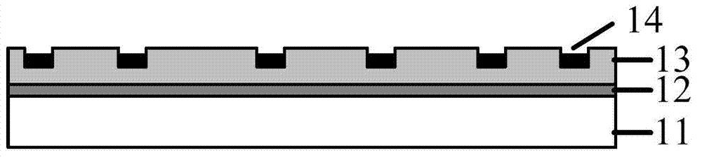
[0031] Please combine figure 1 see Figure 3A-3B , Figure 3A-3B It is a schematic diagram of the transparent conductive film module under the first embodiment of the present invention. The transparent conductive film module includes a first transparent conductive film 41 and a second transparent conductive film 51, both of the first transparent conductive film 41 and the second transparent conductive film 51 are metal-embedded transparent conductive films, combined with figure 1 As shown, the transparent conductive film is the base PET 11 from bottom to top, with a thickness of 188 μm; the acrylic UV glue 13 with a groove structure grid pattern, the groove depth is 3 μm, and the width is 2.2 μm; It is metallic silver 14, the thickness is less than the groove depth, about 2 μm, and the grooves are filled with nano-silver ink and sintered using scrape coating technology. The solid content of silver ink is 35%, and the sintering temperature is 150°C. A layer of adhesion-prom...

Embodiment 2

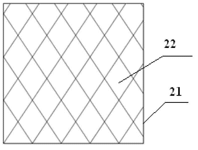
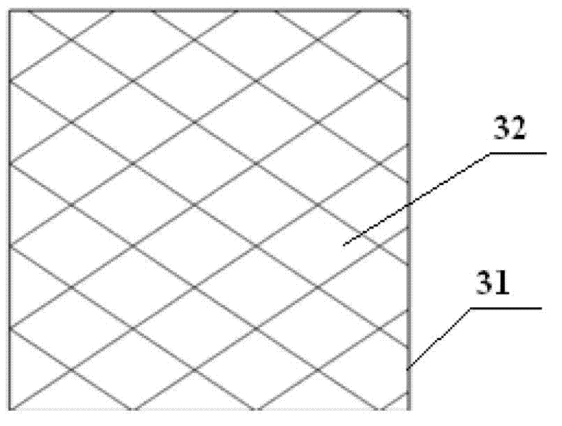
[0037] See Figures 6A-6B , Figures 6A-6B It is a schematic diagram of the transparent conductive film module of the second embodiment of the present invention, such as Figures 6A-6B As shown, the grid 92 of the transparent conductive film 91 is a polygonal random grid composed of metal wires, wherein the distribution probability density of the metal wire slope of the grid along the transverse direction is greater than the distribution probability density along the vertical direction, that is, the slope is close to the X-axis direction The number of metal lines is greater than the metal line whose slope is close to the Y axis; the visible light transmittance of the transparent conductive film 91 is greater than 88.6%; the grid 102 of the transparent conductive film 101 is also a polygonal random grid composed of metal lines, wherein the grid metal lines The distribution probability density of the slope along the longitudinal direction is greater than that along the transver...

Embodiment 3

[0040] Figure 8 , Figure 9 It is a schematic diagram of a transparent conductive film module according to the third embodiment of the present invention. As shown in the figure, in this embodiment, the grid pattern adopts a rectangular grid pattern composed of metal wires. Such as Figure 8 As shown, the surface grid shape of the conductive film 141 is a rectangular grid 142 , and the distribution densities of the metal wires of the rectangular grid 142 along the X and Y axes are different. The conductivity of the conductive film 141 in the X-axis direction is better than that in the Y-axis direction. The slope of most of the metal lines in the grid 142 is distributed at (-1,1). When there are more metal lines distributed in this slope range, the X The better the conductivity in the axial direction. The distribution range of the slope of most grid metal lines in the conductive film 151 is (1,+∞) and (-∞,-1) (not shown in the figure), and the conductivity in the Y-axis dir...


PUM

PropertyMeasurementUnit
widthaaaaaaaaaa
widthaaaaaaaaaa
widthaaaaaaaaaa

Abstract

The invention discloses a transparent conducting film with anisotropic conductivity. The transparent conducting film is suitable for a touch screen, and comprises a first transparent conducing film and a second transparent conducting film, wherein the first transparent conducting film and the second transparent conducting film are embedded metal grid transparent conducting films; in the first transparent conducting film, the probability density of grid metal lines the line slopes of which are close to X axis is larger than the probability density of grid metal lines the line slopes of which are close to Y axis; and in the second transparent conducting film, the probability density of grid metal lines the line slopes of which are close to Y axis is larger than the probability density of grid metal lines the line slopes of which are close to X axis. The transparent conducting film module can ensure constant conductivity while increasing the light transmittance.

Description

technical field [0001] The invention relates to the field of transparent conductive films, in particular to a transparent conductive film with anisotropic conduction. Background technique [0002] The transparent conductive film is a film with good conductivity and high light transmittance in the visible light band. At present, transparent conductive films have been widely used in fields such as flat panel displays, photovoltaic devices, touch panels, and electromagnetic shielding, and have an extremely broad market space. [0003] ITO has been dominating the market for transparent conductive films. However, in most practical applications such as touch screens, multiple processes such as exposure, development, etching, and cleaning are often required to pattern the transparent conductive film, that is, to form fixed conductive areas and insulating areas on the surface of the substrate according to the graphic design. In comparison, using the printing method to directly for...

Claims


Application Information

Patent Timeline
Patent Type & Authority Applications(China)
IPC IPC(8): H01B5/14G06F3/041
CPCH04M1/0266H04M2250/22G06F2203/04103H01B5/14H05K1/0274H05K1/0298H05K2201/0338
Inventor 高育龙崔铮周菲
Owner ANHUI JINGZHUO OPTICAL DISPLAY TECH CO LTD
Why Eureka
Try Eureka