

Epitaxy defect analyzing structure and manufacturing method thereof as well as epitaxy defect analyzing method
A technology for epitaxial defects and manufacturing methods, applied in the fields of semiconductor/solid-state device manufacturing, electrical components, electrical solid-state devices, etc., can solve the problems of incomplete consistency, production capacity, waste of labor, complicated processes, etc., to achieve strong operability and ensure accuracy Sex, the method is simple and fast effect
- Summary
- Abstract
- Description
- Claims
- Application Information
AI Technical Summary
Problems solved by technology
Method used
Image

Examples
Embodiment Construction
[0048] In order to make the above objects, features and advantages of the present invention more comprehensible, specific implementations of the present invention will be described in detail below in conjunction with the accompanying drawings.
[0049] In the following description, numerous specific details are set forth in order to provide a thorough understanding of the present invention. However, the present invention can be implemented in many other ways different from those described here, and those skilled in the art can make similar extensions without violating the connotation of the present invention, so the present invention is not limited by the specific implementations disclosed below.
[0050] The present invention will be further described below in conjunction with specific embodiments and accompanying drawings, but the protection scope of the present invention should not be limited thereby.
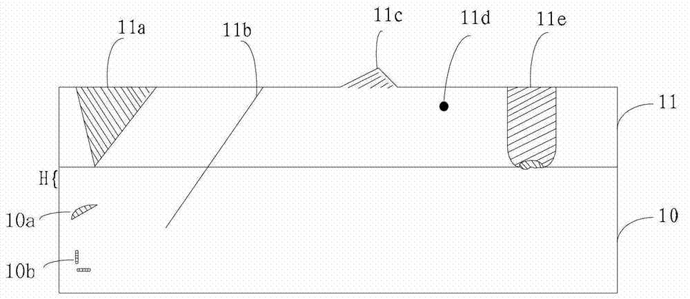
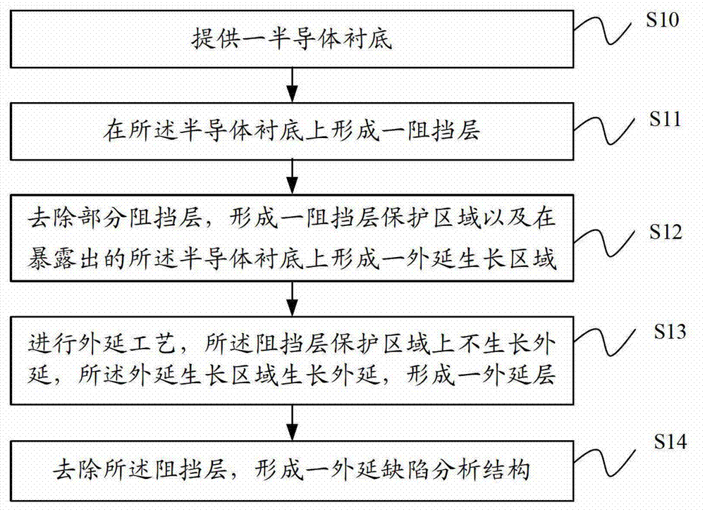
[0051] see figure 2 , the present invention provides a method for man...
PUM
| Property | Measurement | Unit |
|---|---|---|
| Thickness | aaaaa | aaaaa |
Abstract
Description
Claims
Application Information