

SOI device capable of suppressing back gate leakage current caused by radiation and its preparation method
A leakage current and device technology, applied in the field of SOI devices, can solve the problems of SOI device leakage current and device power consumption
- Summary
- Abstract
- Description
- Claims
- Application Information
AI Technical Summary
Problems solved by technology
Method used
Image

Examples
Embodiment Construction
[0029] The implementation of the present invention will be described in detail according to the examples below in conjunction with the accompanying drawings.
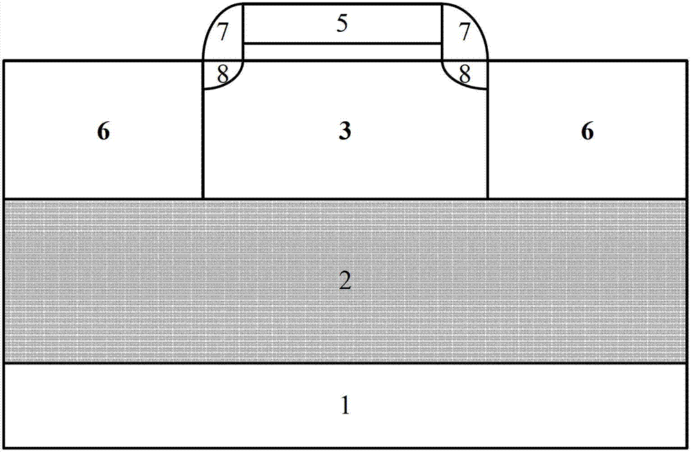
[0030] figure 1 It is a cross-sectional view of an SOI device in the prior art. As shown in the figure, the CMOS device of the present invention includes a substrate 1, a buried oxide layer 2, a semiconductor body region 3, a gate region 5, a source region and a drain region 6, and a gate spacer 7 and LDD area 8.
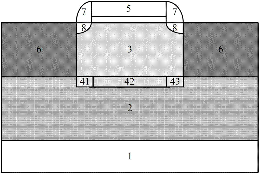
[0031] figure 2 For the sectional view of the SOI device proposed by the present invention, as shown in the figure, the CMOS device of the present invention includes a substrate 1, a buried oxide layer 2, a semiconductor body region 3, an anti-leakage region, a gate region 5, a source region and a drain region 6 , the gate spacer 7 and the LDD region 8 .
[0032] Taking the N-type metal oxide semiconductor NMOS transistor as an example to illustrate the preparation method of the SOI device for suppressing...
PUM
 Abstract
Description
Claims
Application Information