Silicon-on-insulator (SOI) device capable of restraining back gate leakage current caused by radiation and preparation method of SOI device

A leakage current and device technology, applied in the field of SOI devices, can solve the problems of SOI device leakage current and device power consumption

Active Publication Date: 2013-02-20
PEKING UNIV
View PDF5 Cites 2 Cited by
  • Summary
  • Abstract
  • Description
  • Claims
  • Application Information

AI Technical Summary

Problems solved by technology

The ionization damage effect creates a leakage channel in the buried oxide layer of the SOI device, which will increase the off-state leakage current of the SOI device and the power consumption of the device, and will cause a series of reliability problems

Method used


Image

  • Silicon-on-insulator (SOI) device capable of restraining back gate leakage current caused by radiation and preparation method of SOI device
  • Silicon-on-insulator (SOI) device capable of restraining back gate leakage current caused by radiation and preparation method of SOI device
  • Silicon-on-insulator (SOI) device capable of restraining back gate leakage current caused by radiation and preparation method of SOI device

Examples


Embodiment Construction

[0029] The implementation of the present invention will be described in detail according to the examples below in conjunction with the accompanying drawings.

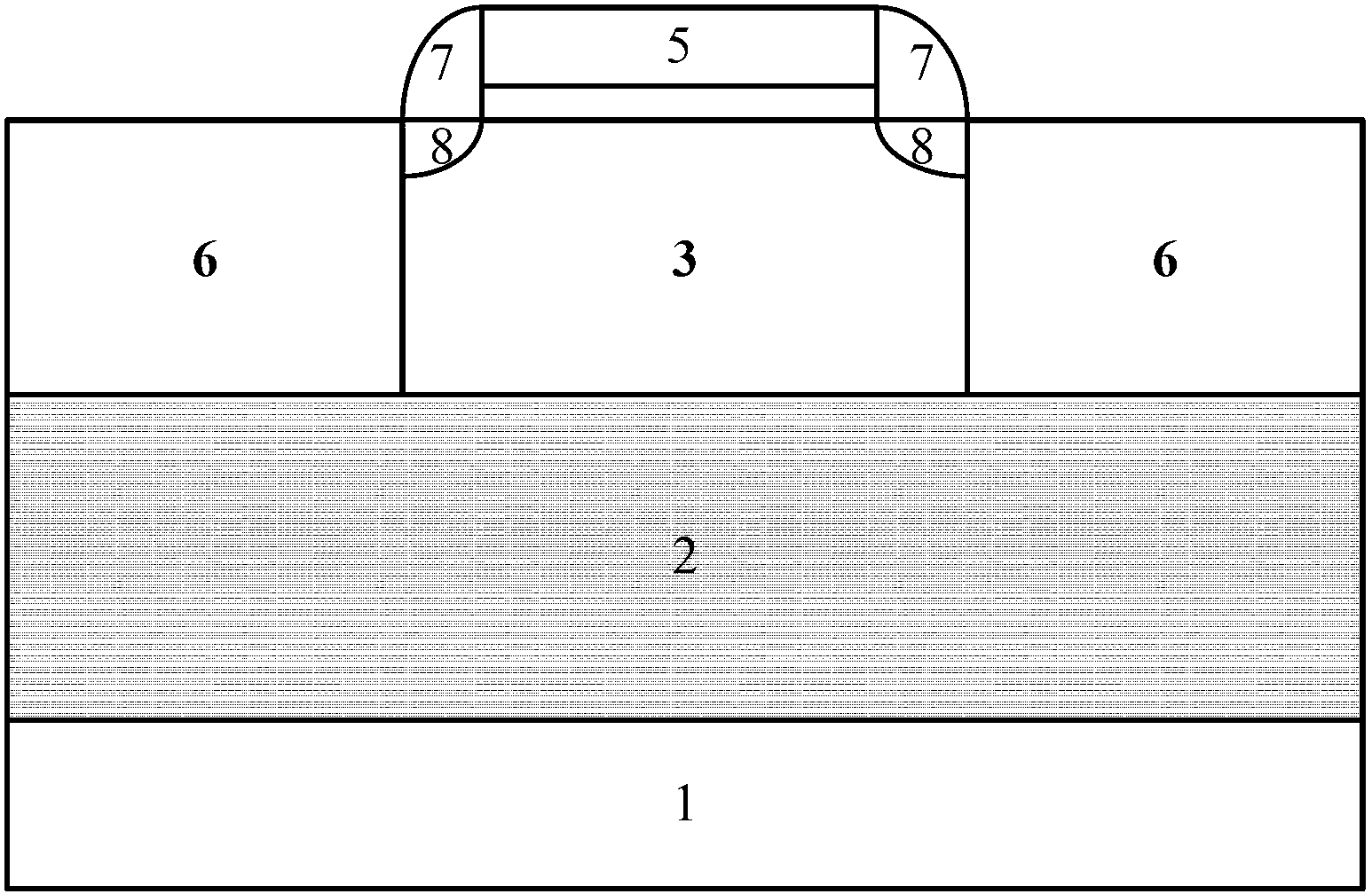
[0030] figure 1 It is a cross-sectional view of an SOI device in the prior art. As shown in the figure, the CMOS device of the present invention includes a substrate 1, a buried oxide layer 2, a semiconductor body region 3, a gate region 5, a source region and a drain region 6, and a gate spacer 7 and LDD area 8.

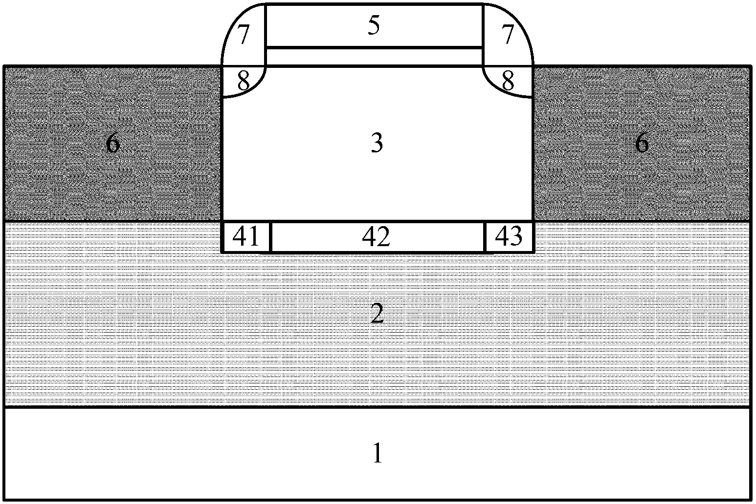
[0031] figure 2 For the sectional view of the SOI device proposed by the present invention, as shown in the figure, the CMOS device of the present invention includes a substrate 1, a buried oxide layer 2, a semiconductor body region 3, an anti-leakage region, a gate region 5, a source region and a drain region 6 , the gate spacer 7 and the LDD region 8 .

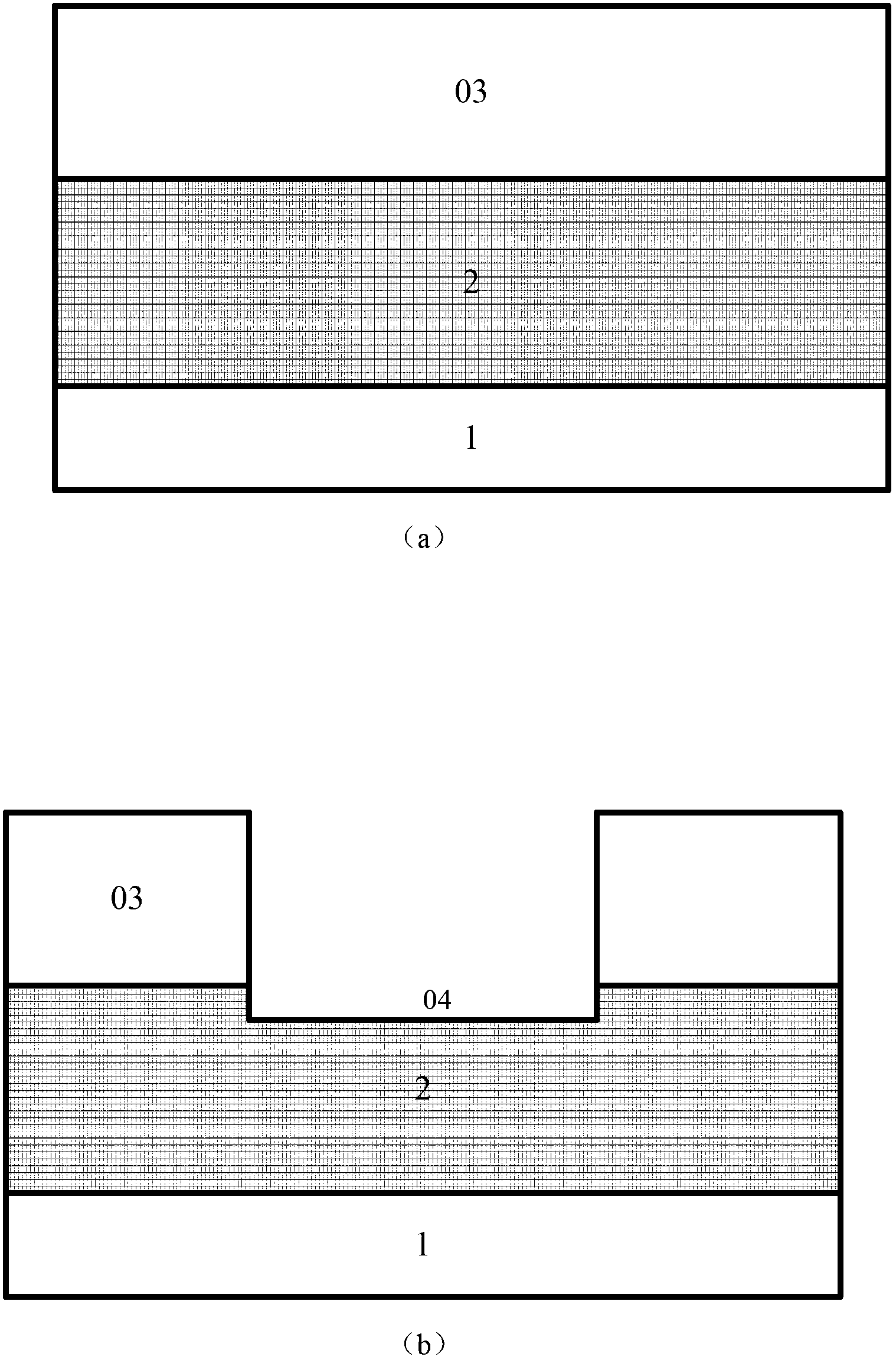
[0032] Taking the N-type metal oxide semiconductor NMOS transistor as an example to illustrate the preparation method of the SOI device for suppressing...


PUM

PropertyMeasurementUnit
Thicknessaaaaaaaaaa

Abstract

The invention discloses an SOI device capable of restraining back gate leakage current caused by radiation and a preparation method of the SOI device. The SOI device comprises a substrate, a buried oxide layer, a semiconductor body region, a grid region, a source region, a drain region, a grid side wall, a lightly doped drain (LDD) region and a leakproof region, wherein the leakproof region is sunk in the buried oxide layer and is located below the semiconductor body region. According to the photoetching SOI device, the buried oxide layer forms a sunk region, a semiconductor material is grown in an epitaxial mode and is doped regionally to form the leakproof region, the second portion in the middle is a heavily-doped region and is not easily radiated by positively charged trapped charge transoid formed by buried oxide, the back gate leakage current of the SOI device, which is caused by radiation, can be effectively restrained, and the reliability of the SOI device in a radiation environment is improved. According to the SOI device and the preparation method, only conventional processes such as photoetching, epitaxy and ion implantation doping are introduced during preparation of the conventional SOI device, so that the process is simple and compatible with existing technologies.

Description

technical field [0001] The invention relates to an SOI device, in particular to an SOI device capable of suppressing back gate leakage current caused by radiation and a preparation method thereof. Background technique [0002] Silicon-On-Insulator (Silicon-On-Insulator) SOI introduces a buried oxide layer between the top layer of silicon and the substrate, so that SOI field effect transistors have smaller parasitic capacitance and higher device performance than traditional bulk silicon devices. The advantage of low power consumption, and the SOI device eliminates the latch-up effect, has extremely broad application prospects in the fields of high-performance ultra-large integrated circuits, high-speed storage devices, low-power circuits, and high-temperature sensors. SOI devices in the prior art include: a substrate, a buried oxide layer, a semiconductor body region, a gate region, a source region and a drain region, a gate spacer and a lightly doped drain LDD region; wherei...

Claims


Application Information

Patent Timeline
IPC IPC(8): H01L29/78H01L29/06H01L21/336
Inventor 黄如谭斐安霞黄良喜武唯康张兴
Owner PEKING UNIV
Why Eureka
Try Eureka