Method for reducing area of interconnected input-output pins on stacked chips

A technology of input and output pins, which is applied in the field of reducing the area of ​​interconnected input and output pins on stacked chips, can solve the problems of strong anti-static discharge capability, large driving capability, and large area, so as to reduce chip cost and reduce Chip area, the effect of reducing the area of ​​interconnection input and output pins

Active Publication Date: 2013-02-27
SHANGHAI XINCHU INTEGRATED CIRCUIT
View PDF4 Cites 3 Cited by
  • Summary
  • Abstract
  • Description
  • Claims
  • Application Information

AI Technical Summary

Problems solved by technology

[0004] The invention overcomes the problems in the background technology that the driving capability of the interconnection pins in the stacked chips is too large and the antistatic discharge ability is too strong, which leads to the problem that the area of ​​the interconnection output and input pins between the stacked chips is too large, and proposes a method for reducing stacking Method for interconnecting input and output pin areas on a chip

Method used


Image

  • Method for reducing area of interconnected input-output pins on stacked chips
  • Method for reducing area of interconnected input-output pins on stacked chips
  • Method for reducing area of interconnected input-output pins on stacked chips

Examples


Embodiment 1

[0027] In this embodiment, by reducing the driving capability of the interconnected input and output pins on the upper and lower stacked chips with the microcontroller standard system bus as the pin interconnection and reducing the performance of its electrostatic discharge protection, thereby reducing its interconnection The size of the output and input pin area, and the size of multiple chips stacked up and down using the microcontroller standard system bus for pin interconnection are further reduced, which further reduces the cost of the SOC chip.

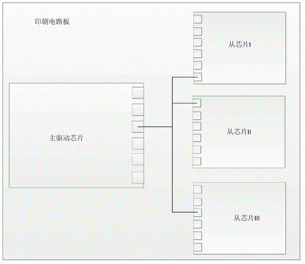
[0028] figure 2 Shown is a generic PCB with a master driver chip and 3 slave chips on top of it. One output pin of the main driver chip is connected to the input pins of the three slave chips to drive three slave chips at the same time, so for the output pin on the main driver chip, its driving capability must be Very large, for example, the driving current is above 20mA. But for multiple chips stacked up and down using the s...

Embodiment 2

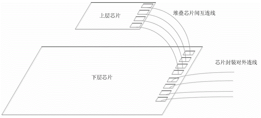
[0032] The interconnection pins of the upper chip in the present invention are not directly connected to the pins of the package shell after the packaging is completed, so the probability of ESD occurring on the upper chip and the requirements for ESD will be reduced. After packaging, the ESD of the whole chip is determined by the ESD performance of the underlying chip. Therefore, on the premise of not reducing the final ESD performance of the chip, the ESD requirements can be reduced by reducing the single transistor size or number of the upper chip ESD transistors (including MOS transistors, diodes or other ESD antistatic structures).

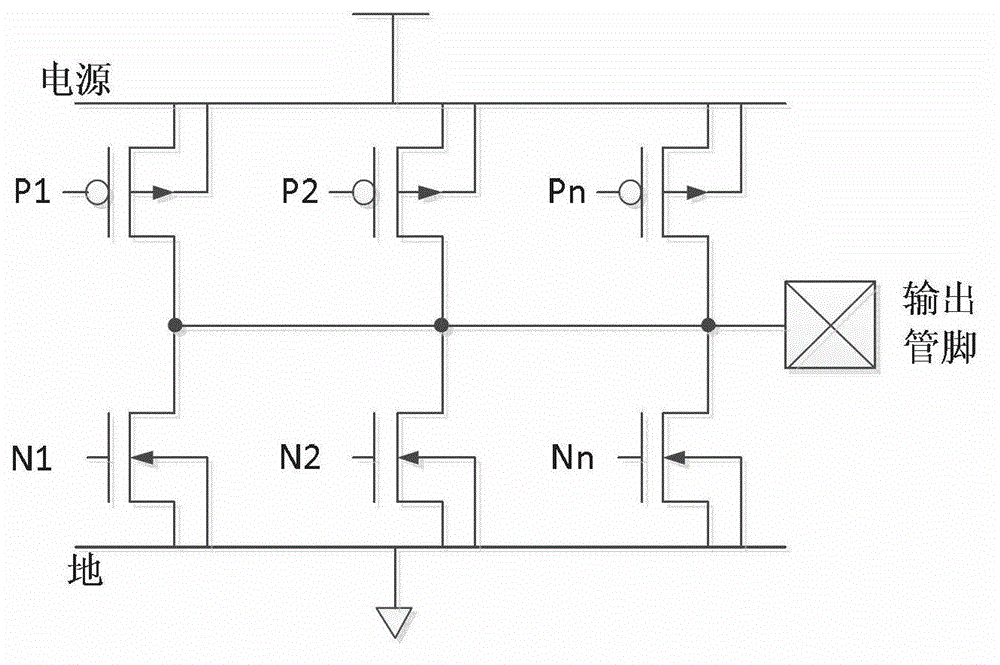
[0033] For example, if the usual HBM 2000V is reduced to HBM 500V, the area of ​​the ESD part of the upper chip can be reduced to a quarter of the original.

[0034] For example, the original ESD transistor that can withstand HBM2000V is composed of 12 NMOS transistors with a width of 30um and a length of 0.45um and 20 PMOS transistors with a...


PUM


Abstract

The invention discloses a method for reducing the area of interconnected input-output pins on stacked chips. In the manufacturing process of the stacked chips, the area of the interconnected input-output pins is reduced by reducing the number and size of driving transistors in the interconnected input-output pins and reducing the number and size of anti-static discharge devices transistors in the interconnected input-output pins, wherein the stacked chips are interconnected by microcontroller standard system buses as pins. According to the invention, the area of the interconnected input-output pins is reduced by reducing the size of the driving circuit and the size of the anti-static discharge circuit in the interconnected input-output pins on the plurality of chips stacked up and down and interconnected by microcontroller standard system bus as pins, and reducing the number of the driving circuit transistor and the number of the anti-static discharge circuit transistor, as a result, the area of the chip is reduced and the cost of the chip is reduced.

Description

technical field [0001] The invention relates to the technical field of chip stacking, in particular to a method for reducing the area of ​​interconnection input and output pins on stacked chips. Background technique [0002] Since the digital and analog circuits cannot be scaled down simultaneously with the continuous reduction of the size of the integrated circuit manufacturing process, when the technology is getting more and more advanced, the digital-analog hybrid system-on-chip can be implemented on the same chip with the same technology. Costs will become less and less optimized. Now based on the chip stacking technology, the digital logic unit and the analog circuit in the system on chip are separated, and the digital logic unit whose area can be reduced proportionally with the continuous reduction of the process size is realized on the advanced small-size process chip, and the area cannot be reduced. With the continuous shrinking of process size and proportional redu...

Claims


Application Information

Patent Timeline
Patent Type & Authority Applications(China)
IPC IPC(8): H01L21/768
Inventor 景蔚亮陈邦明亢勇
Owner SHANGHAI XINCHU INTEGRATED CIRCUIT
Why Eureka
Try Eureka