Circuit board mark detection and offset detection method and arrangement method
A circuit board and offset technology, applied in the field of mark detection and offset detection, can solve the problems of bad sub-board detection, long idle time, etc., and achieve the effect of shortening the output time
- Summary
- Abstract
- Description
- Claims
- Application Information
AI Technical Summary
Problems solved by technology
Method used
Image

Examples
Embodiment Construction
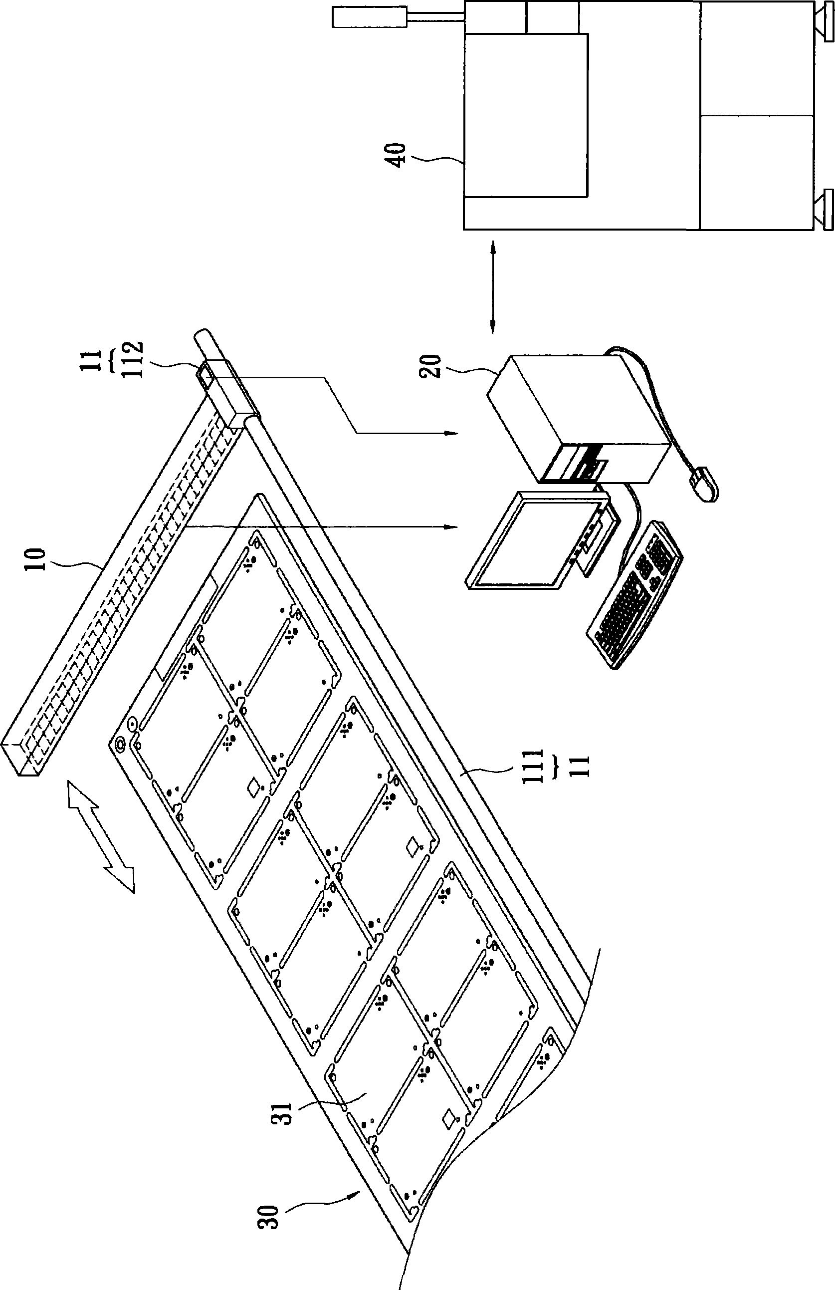
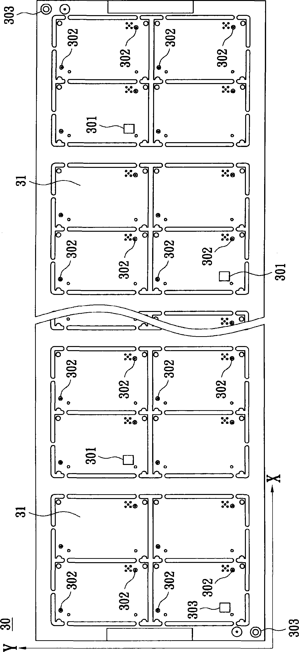
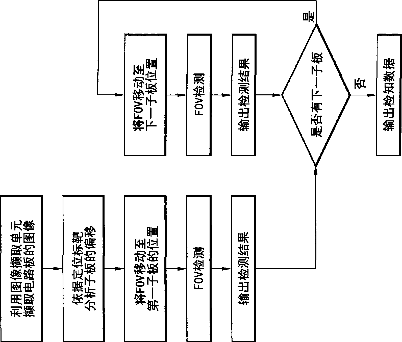
[0022] The present invention is to provide a detection device independent of the component mounting machine upstream of the component mounting machine (such as the pick-and-place machine, flip-up component machine: Flip Chip Mounter), which is used to quickly and independently detect the circuit Bad marks or / and local fiducial marks on multiple sub-boards on the board, and passed to the downstream pick-and-place machine, so that the subsequent part-placement steps can be based on the detection device of the mark The obtained detection data is placed on the sub-boards belonging to good products, so that the standby time of the pick-and-place machine (including film feeding, film output, target detection time and detection time of defective product marks) is greatly shortened, It is not necessary to perform this detection operation on the part placement machine, thereby increasing the productivity of the overall production line. Moreover, the detection device of the present inve...
PUM
 Abstract
Description
Claims
Application Information