Method for forming wire in semiconductor device

Inactive Publication Date: 2002-11-28
CONVERSANT INTPROP MANAGEMENT INC
View PDF0 Cites 4 Cited by
  • Summary
  • Abstract
  • Description
  • Claims
  • Application Information

AI Technical Summary

Benefits of technology

0012] Therefore, a method for forming a wire in a semiconductor device is disclosed, wherein, in forming a titanium film and a titanium nitride film as a barrier metal layer, the titanium film and a titanium nitride film are deposited in different chambers by removing a titanium oxide film used as an insulating film that is generated by an upper titanium portion of a titanium layer bondi

Problems solved by technology

However, the cluster of equipment consisting of multi-chambers in ultra high vacuum is very expensive and the construction of the cluster of equipment is made complex

Method used


Image

  • Method for forming wire in semiconductor device
  • Method for forming wire in semiconductor device
  • Method for forming wire in semiconductor device

Examples


Embodiment Construction

[0018] The disclosed methods will now be described with reference to the accompanying drawings.

[0019] FIGS. 2a through 2e are cross-sectional views sequentially illustrating a method for forming a wire in a semiconductor device.

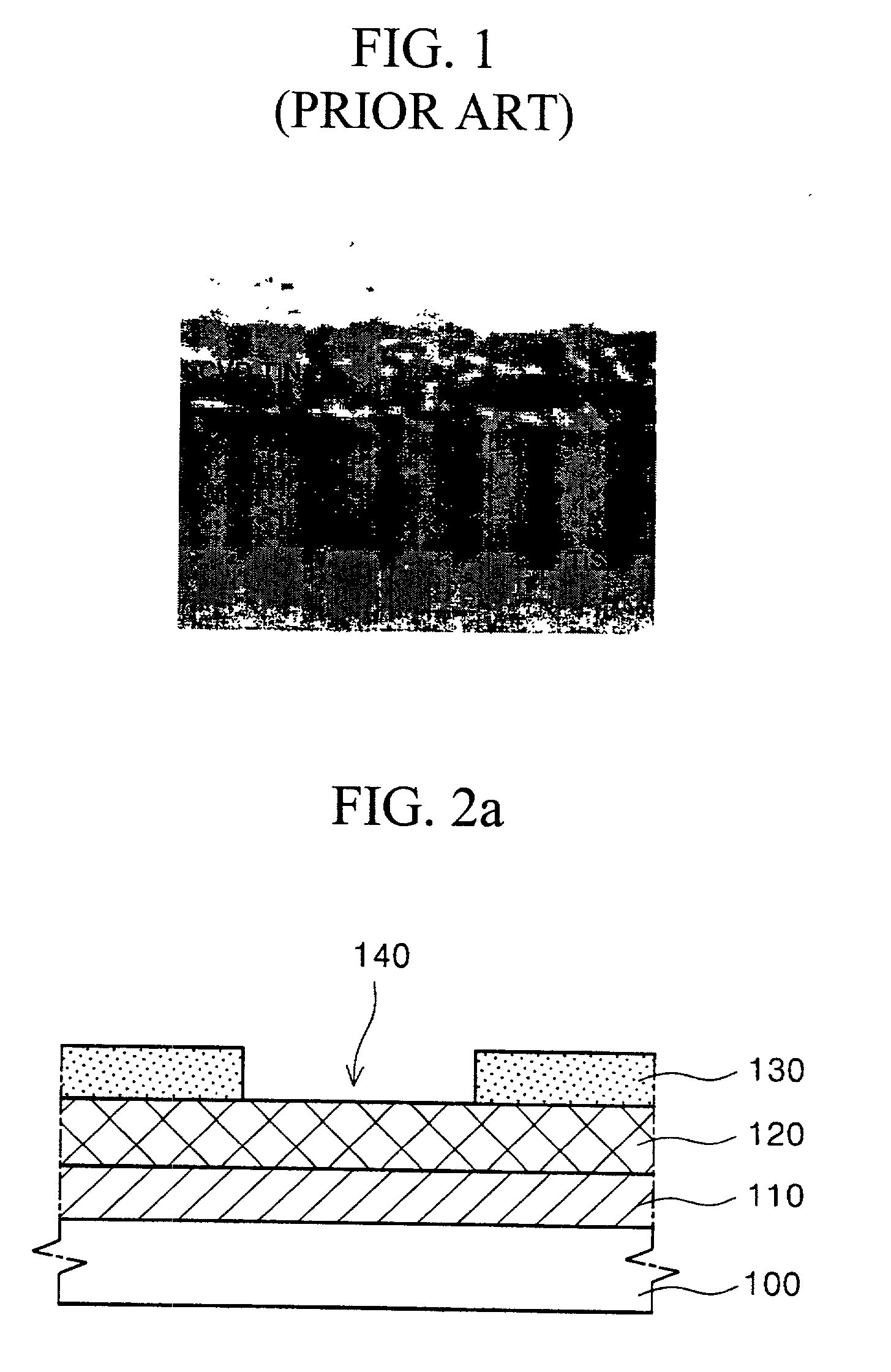
[0020] As illustrated in FIG. 2a, a conductive layer 110 and a dielectric layer 120 are sequentially deposited on a semiconductor substrate 100 having a predetermined lower substructure, and then a photoresist film 130 is coated thereon, for thereby forming a contact hole forming portion 140.

[0021] At this time, titanium (Ti) silicide or cobalt (Co) silicide is adapted as the conductive layer 110, and the silicide can be formed by a silicide method.

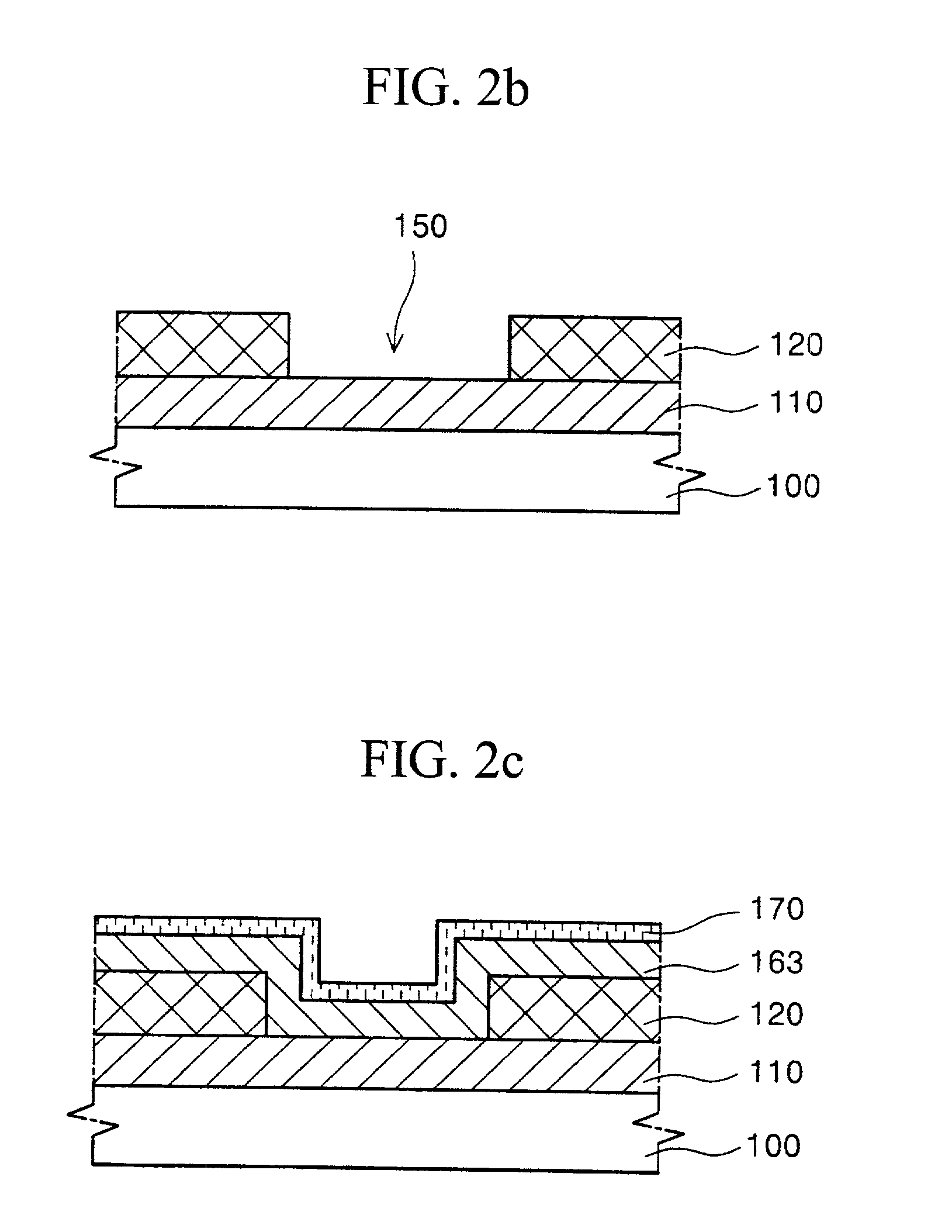
[0022] Continuously, as illustrated in FIG. 2b, a contact hole 150 is formed in the dielectric layer 120 by performing an etching process for etching the dielectric layer 120 up to the upper part of the lower conductive layer 110 using the photoresist film 130 as a mask.

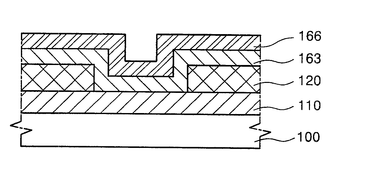
[0023] Then, as illustrated in FIG. 2c, titan...


PUM


Abstract

A method for forming a wire in a semiconductor device, in forming a titanium film and a titanium nitride film as a barrier metal layer, which can deposit a titanium film and a titanium nitride film each in a different chamber by removing a titanium oxide film used as an insulating film made of upper titanium bonding with oxygen in air as the upper portion of a titanium film is exposed to air by a plasma process and then depositing a titanium nitride film, and as a result can reduce the throughput time of chamber equipment since the partial utilization of the system of the chamber equipment is enabled by driving another chamber even in case one of the chambers breaks down.

Description

BACKGROUND[0001] 1. Technical Field[0002] A method for forming a wire in a semiconductor device is disclosed. More particularly, a method for forming a wire in a semiconductor device is disclosed, wherein in forming a titanium film and a titanium nitride film as a barrier metal layer, a titanium film and a titanium nitride film are each deposited in different chambers by first removing a titanium oxide film that is used as an insulating film. The titanium oxide film is generated by allowing the upper titanium portion of the titanium film to bond with oxygen in air as the upper portion of a titanium film is exposed to air by a plasma process. A titanium nitride film is then deposited on the underlying non-oxidated titanium film. The disclosed methods reduce the throughput time of each chamber even in the case where one chamber breaks down.[0003] 2. Description of the Related Art[0004] Generally, in the method for fabricating a semiconductor device, on condition that a metal wire serv...

Claims


Application Information

Patent Timeline
IPC IPC(8): H01L21/28H01L21/3205H01L21/3213H01L21/768H01L23/52
CPCH01L21/32136H01L21/76862H01L21/76843H01L21/28
Inventor CHO, YOUNG-A
Owner CONVERSANT INTPROP MANAGEMENT INC
Why Eureka
Try Eureka