Array substrate, display module and preparation method for array substrate

An array substrate and substrate technology, applied in semiconductor/solid-state device manufacturing, optics, instruments, etc., can solve the problems of low transmittance of metal materials, low aperture ratio of pixel units, and affecting the brightness of liquid crystal displays, etc., to improve brightness and increase The effect of aperture ratio

Active Publication Date: 2013-03-20
BOE TECH GRP CO LTD +1
View PDF5 Cites 12 Cited by
  • Summary
  • Abstract
  • Description
  • Claims
  • Application Information

AI Technical Summary

Problems solved by technology

[0003] Existing TFT-LCDs include various types, among them, Advanced super Dimension Switch (hereinafter referred to as ADS) type and in-plane switching (In-Plane Switching, hereinafter referred to as IPS) type TFT-LCD Among them, the common electrode and the common electrode line are usually arranged on the same layer as the gate, and are made of the same metal material as the gate. Due to the low transmittance of the metal material, the aperture ratio of the pixel unit is low, which affects the liquid crystal. display brightness

Method used


Image

  • Array substrate, display module and preparation method for array substrate
  • Array substrate, display module and preparation method for array substrate
  • Array substrate, display module and preparation method for array substrate

Examples


Embodiment 1

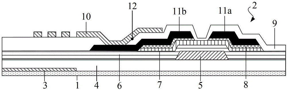
[0024] The invention provides an array substrate, such as figure 1 As shown, including substrate 1, TFT2, gate lines (not shown in the figure) and data lines (not shown in the figure), the gate lines and data lines are surrounded to form a plurality of pixel units, and each pixel unit is formed with a transparent common The electrode 3 and the TFT2 are formed on the transparent common electrode 3 , and an insulating layer 4 is formed between the TFT2 and the transparent common electrode 3 .

[0025] The TFT2 includes: a gate 5 formed on the insulating layer 4; a gate insulating layer 6 covering the gate line, the gate 5 and the insulating layer 4; an active layer 7 corresponding to the gate 5 on the gate insulating layer 6 , ohmic contact layer 8, source electrode 11a, drain electrode 11b, source-drain insulating layer 9 and pixel electrode 10, wherein the material of active layer 7 is amorphous silicon, and the material of ohmic contact layer 8 is amorphous silicon doped with...

Embodiment 2

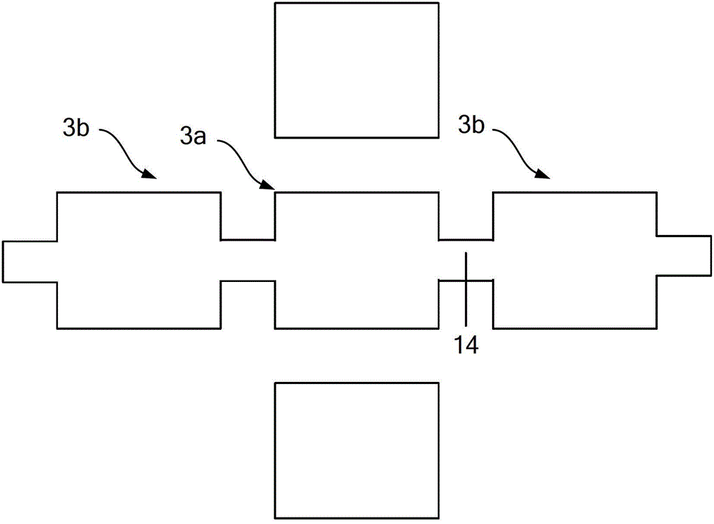
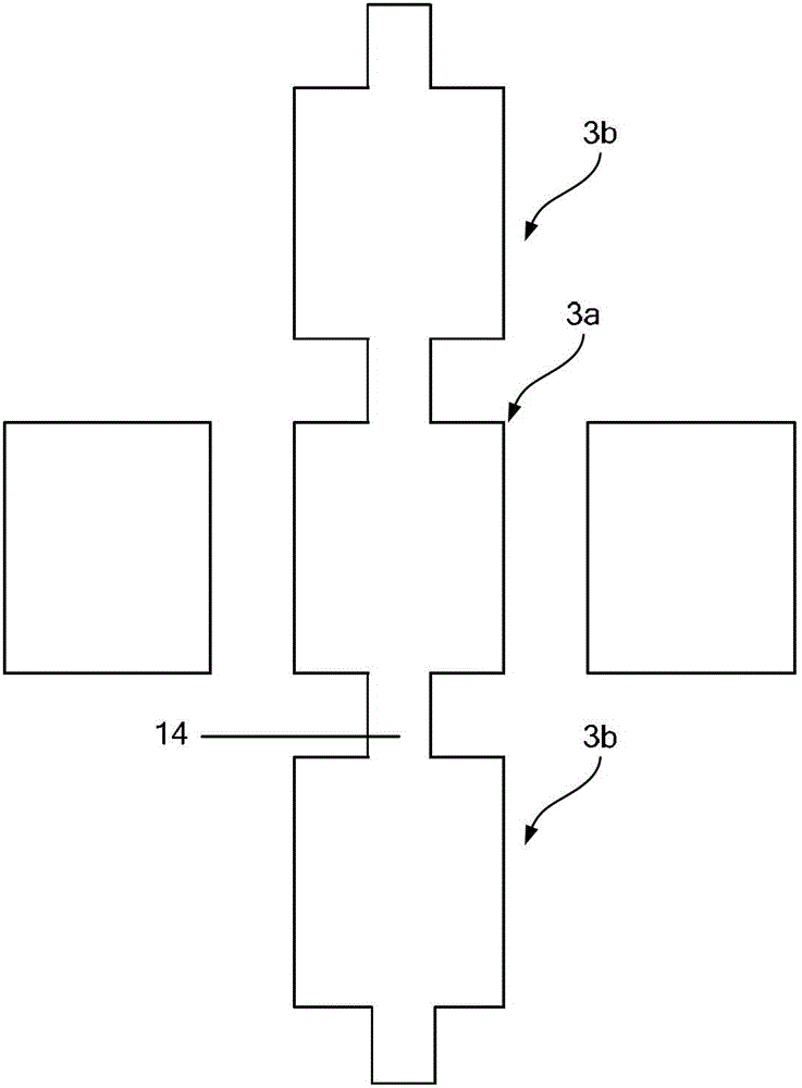
[0033] In the above-mentioned embodiments, the common electrode lines 13 still need to be provided on the substrate 1 , which makes the formed pattern more complicated, and uses more conductive materials, resulting in waste.

[0034] In order to solve the above problems, preferably, such as figure 2 As shown, the transparent common electrode 3a on the substrate 1 is connected to the transparent common electrode 3b of the adjacent pixel unit through the connection line 14; correspondingly, the common electrode line can only be arranged at the transparent common electrode 3b at the edge of the array substrate; , the control circuit first charges the outermost transparent common electrode through the common electrode line, and the outermost transparent common electrode charges the adjacent transparent common electrode through the connection line 14, so as to charge all the transparent common electrodes 3, and further proceed evenly.

[0035] Specifically, such as figure 2 As ...

Embodiment 3

[0043] Corresponding to the array substrate described in Embodiment 1 and Embodiment 2, the present invention also provides a display module, including the above-mentioned array substrate, the array substrate,

[0044] Such as figure 1 As shown, it includes a substrate 1, TFT2, gate lines and data lines. The gate lines and data lines are surrounded to form a plurality of pixel units, and each pixel unit is formed with a transparent common electrode 3. TFT2 is formed on the transparent common electrode 3. TFT2 and An insulating layer 4 is formed between the transparent common electrodes 3 .

[0045] The TFT2 includes: a gate line and a gate 5 formed on the insulating layer 4; a gate insulating layer 6 covering the gate line, the gate 5 and the insulating layer 4; Source layer 7, ohmic contact layer 8, data line, source electrode 11a, drain electrode 11b, source-drain insulating layer 9 and pixel electrode 10, wherein the material of active layer 7 is amorphous silicon, and the...


PUM


Abstract

The invention discloses an array substrate, a display module and a preparation method for the array substrate and belongs to the field of display. The array substrate is designed so as to solve the problems that width occupied by a common electrode wire and a grid line is excessively large and the aperture opening ratio of every pixel cell is reduced. The array substrate comprises a thin film transistor, the grid line and a data line, wherein the grid line and the data line are encircled to form a plurality of pixel cells. A transparent common electrode is formed on each pixel cell; the thin film transistor is formed on the transparent common electrodes; and an insulating layer is formed between the thin film transistor and the transparent common electrodes.

Description

technical field [0001] The invention relates to the display field, in particular to an array substrate, a display module and a preparation method thereof. Background technique [0002] Thin Film Transistor-Liquid Crystal Display (hereinafter referred to as TFT-LCD) has the advantages of light weight, thin thickness and low power consumption, and is widely used in electronic products such as TVs, mobile phones and monitors. [0003] Existing TFT-LCDs include various types, among them, Advanced super Dimension Switch (hereinafter referred to as ADS) type and in-plane switching (In-Plane Switching, hereinafter referred to as IPS) type TFT-LCD Among them, the common electrode and the common electrode line are usually arranged on the same layer as the gate, and are made of the same metal material as the gate. Due to the low transmittance of the metal material, the aperture ratio of the pixel unit is low, which affects the liquid crystal. The brightness of the display. Contents...

Claims


Application Information

Patent Timeline
Patent Type & Authority Applications(China)
IPC IPC(8): G02F1/1362G02F1/1368G02F1/1343H01L27/12H01L21/77
Inventor 郤玉生林鸿涛白金超
Owner BOE TECH GRP CO LTD
Why Eureka
Try Eureka