TEM Sample Carrier

A technology of transmission electron microscope samples and carrying devices, which is applied in the directions of circuits, discharge tubes, electrical components, etc., can solve the problems of high equipment requirements, high requirements, affecting high-resolution structural information, etc., and achieves the effect of high integration.

Inactive Publication Date: 2015-07-29
PEKING UNIV
View PDF4 Cites 3 Cited by
  • Summary
  • Abstract
  • Description
  • Claims
  • Application Information

AI Technical Summary

Problems solved by technology

However, this structure has high requirements on silicon wafer processing technology and equipment, and will affect the acquisition of high-resolution structural information of samples.

Method used


Image

  • TEM Sample Carrier
  • TEM Sample Carrier
  • TEM Sample Carrier

Examples


Embodiment Construction

[0021] The present invention will be further described below in conjunction with the drawings, but it is not limited thereto.

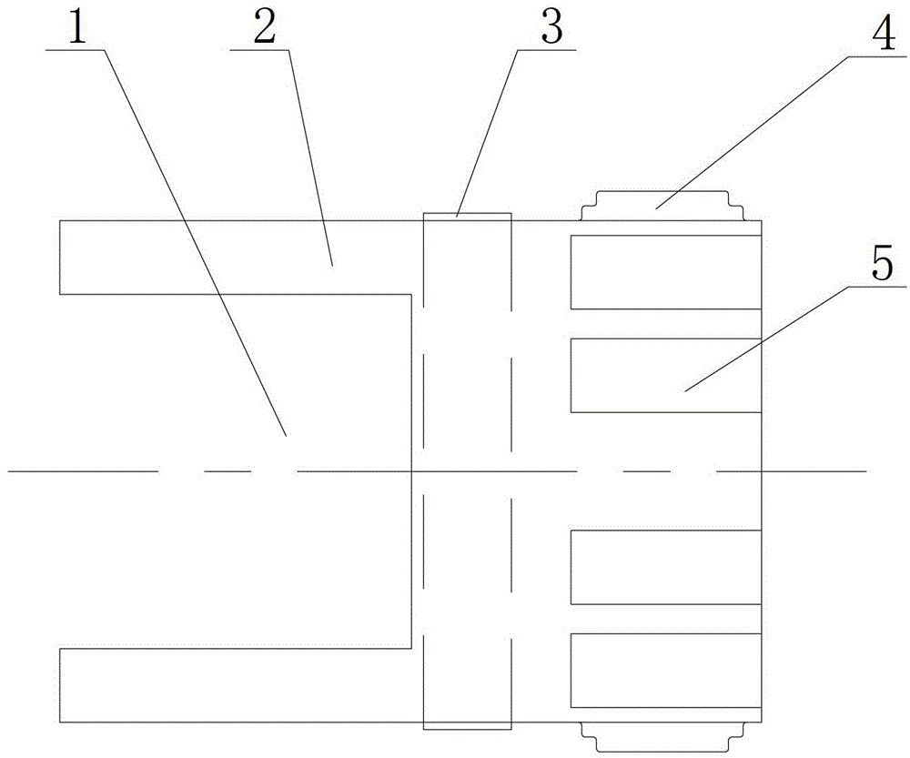
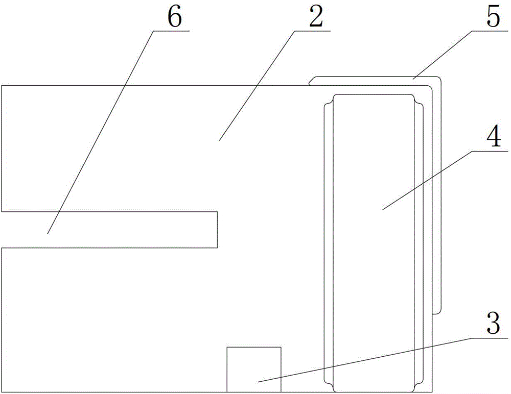
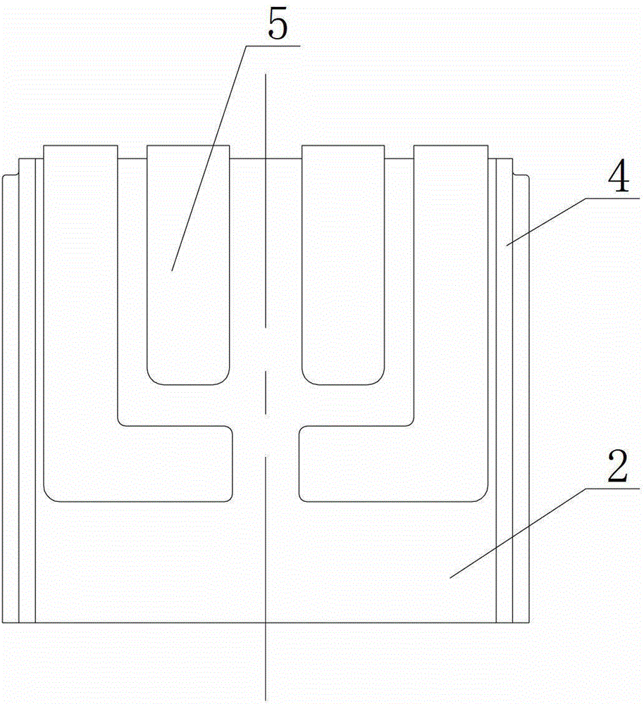
[0022] Such as figure 1 As shown, the structure of the present invention mainly includes a supporting part 2 and a metal electrode 5. The carrying part 2 is used to carry the nano device substrate, and a through hole 1 is opened on one side of the carrying part 2, and the electron beam can pass through the through hole 1 to hit the sample on the nano device substrate on the carrying part 2. At the same time, The detection probe can also be easily moved from the through hole 1 to the edge of the substrate to bend, modify, change the contact and other operations of the sample; the center of the through hole 1 should be close to the center of the field of view of the transmission electron microscope to maximize the sample stage Field of view in X, Y, and Z directions. in figure 1 In this case, the shape of the through hole 1 is rectangular, but it can also...


PUM


Abstract

The invention provides a transmission electron microscope sample bearing device which comprises a bearing portion and metal electrodes. Structures of a through hole, a clamp groove, a metal sheet / layer and the like are arranged at the bearing portion. The bearing portion can bear samples with the size identical with micro grids and the thickness smaller than or equal to 500mum. When sample substrates are fixed, a detection probe can be further conveniently moved from the through hole at the edges of the samples to carry out bending, decoration, contact change and the like on the samples. Furthermore, a transmission electron microscope is used for observing. The metal electrodes can be connected with source electrodes, leakage electrodes and grid electrodes of nanometer components in the samples. By means of an external power supply and an instrument, nanometer electron components can be measured in an in-situ mode. The metal sheet / layer of the bearing portion can effectively eliminate electrostatic interference.

Description

Technical field [0001] The invention relates to a physical device, in particular to a transmission electron microscope sample carrying device, which can be used to realize in-situ measurement of nano electronic devices in the transmission electron microscope. Background technique [0002] Compared with macroscopic materials, nanomaterials have a small size and a large surface-to-volume ratio, exhibiting unique quantum effects and surface effects, especially the unique structure of one-dimensional or quasi-one-dimensional nanomaterials makes it a The device has a very large potential advantage. Nanoelectronic devices are becoming an important breakthrough to solve the problem of the size reduction limit of traditional microelectronic devices; the research work of nanodevices in high-performance optoelectronic devices, sensors and various new principles and new functional devices has also continuously achieved important results. The performance of nanodevices is directly affected ...

Claims


Application Information

Patent Timeline
Patent Type & Authority Patents(China)
IPC IPC(8): H01J37/20H01J37/26
Inventor 许婷婷陈清
Owner PEKING UNIV
Why Eureka
Try Eureka