Supercharge Your Innovation With Domain-Expert AI Agents!

Impedance matching element

A technology of impedance matching and components, applied in the direction of impedance network, electrical components, transformer/inductance parts, etc.

Inactive Publication Date: 2013-03-20
NGK INSULATORS LTD
View PDF7 Cites 4 Cited by
  • Summary
  • Abstract
  • Description
  • Claims
  • Application Information

AI Technical Summary

Problems solved by technology

[0016] The present invention was created to solve the aforementioned problems related to impedance matching circuits.

Method used


Image

  • Impedance matching element
  • Impedance matching element

Examples


Embodiment

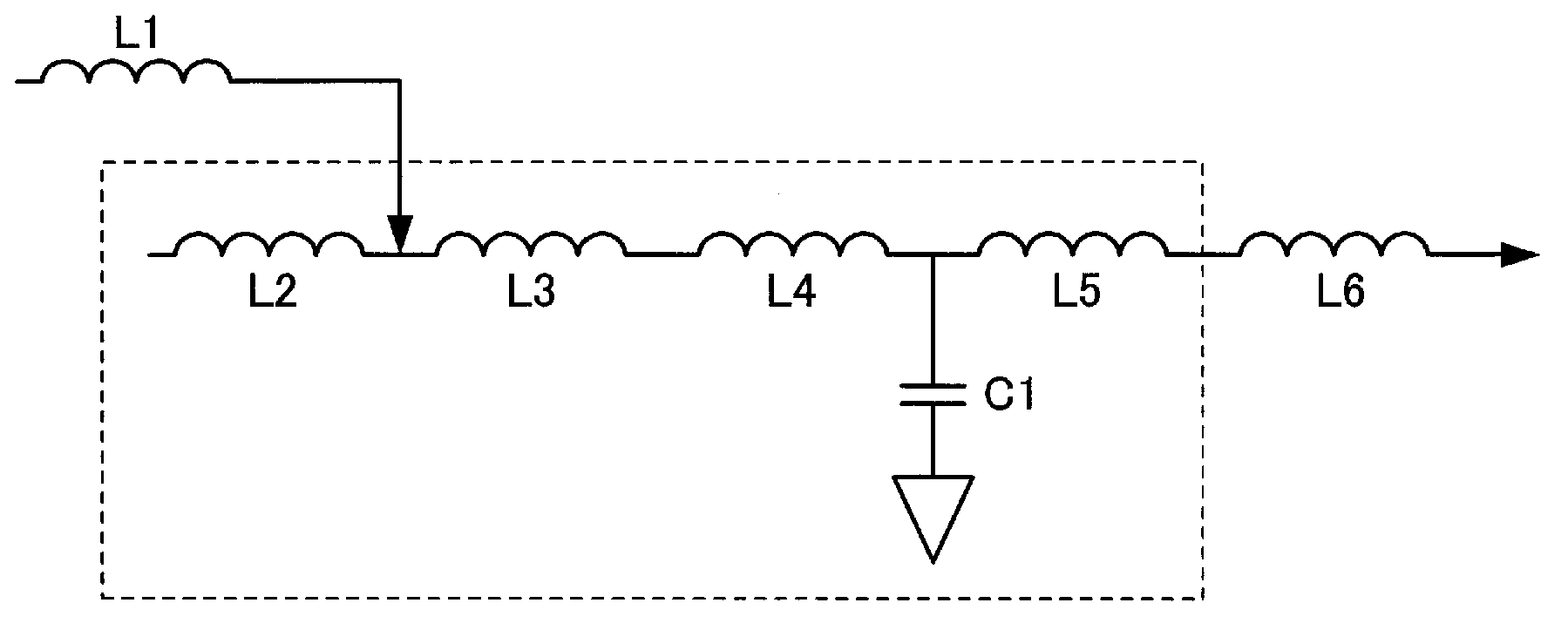
[0095] (1) Explanation based on equivalent circuit

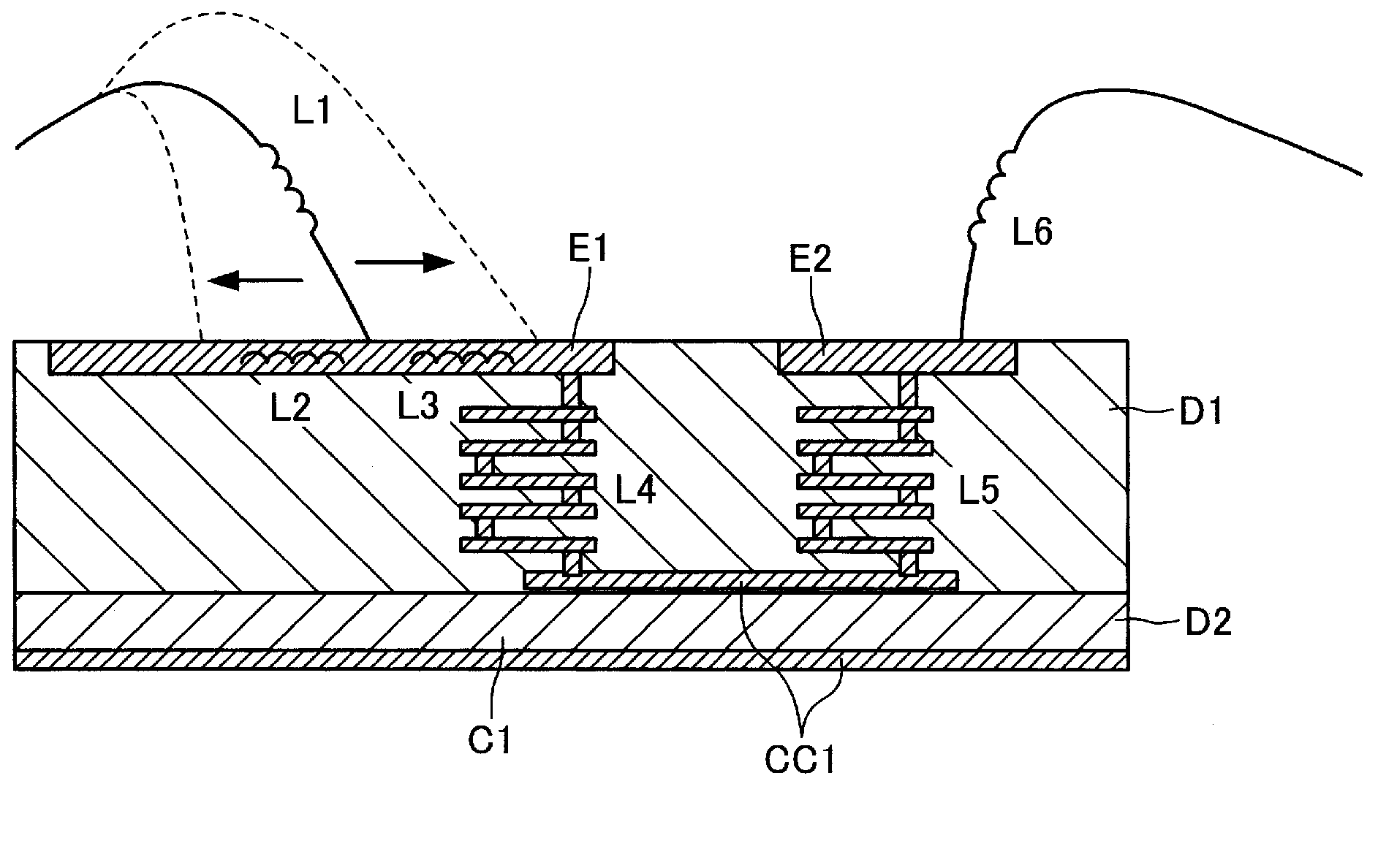
[0096] figure 1 It is an equivalent circuit diagram showing the configuration of the impedance matching element of this embodiment. exist figure 1 In , the constituent elements inside the quadrangular frame depicted by dotted lines indicate the constituent elements included in the impedance matching element of this embodiment. That is, in figure 1 Among them, L1 and L6 are structural elements not included in the impedance matching element of this embodiment, and specifically represent the components used to connect the impedance matching element of this embodiment to other elements (for example, external circuits such as high-frequency semiconductor amplifying elements). metallic line.

[0097] On the other hand, L4 and L5 represent the first dielectric material D1 ( figure 1 not shown in the internal inductor section. The capacitor part C1 is connected to the portion connecting the inductor parts L4 and L5, and the ot...


PUM


Abstract

The objective is to provide a miniature impedance matching element wherein unevenness in quality is low and which has high current tolerance. The objective is achieved by an impedance matching element provided with a wiring portion including a wiring-use conductor pattern embedded in an interior or formed upon a surface of a first dielectric material (D1); and inductor units (L4 and L5) including an inductor-use conductor pattern embedded in the interior or formed upon the surface of the first dielectric material (D1); and / or a capacitor portion (C1) including at least one pair of capacitor-use conductor patterns (CC1) and a second dielectric material (D2) which interposes between the pair of capacitor-use conductor patterns and which has a higher dielectric constant than the first dielectric material (D1); wherein the impedance matching element is such that the thicknesses of the wiring-use conductor pattern and the inductor-use conductor pattern are greater than or equal to 20 [mu]m.

Description

technical field [0001] The present invention relates to impedance matching elements. More specifically, the present invention relates to a small-sized impedance matching element with small variation in quality and high current tolerance. Background technique [0002] In general, semiconductor elements including silicon (Si), gallium nitride (GaN), and the like have low output impedance, and therefore are often connected to an impedance matching circuit when connected to an external circuit. By connecting to an impedance matching circuit, the characteristic impedance of the external circuit can be matched, and the output from the semiconductor element can be sent to the external circuit without waste. [0003] The above-mentioned impedance matching circuit is often composed of a capacitor element and an inductor element formed of a thin conductor wire (for example, a metal wire) connecting the capacitor element and the semiconductor element as described above. In this confi...

Claims


Application Information

Patent Timeline
Patent Type & Authority Applications(China)
IPC IPC(8): H03H7/38H01F27/00
CPCH03H7/38H01F2017/0026H01F17/02
Inventor 平井隆己滑川政彦矢野信介
Owner NGK INSULATORS LTD
Features
  • R&D
  • Intellectual Property
  • Life Sciences
  • Materials
  • Tech Scout
  • Unparalleled Data Quality
  • Higher Quality Content
  • 60% Fewer Hallucinations
Learn More