Inverted laser chip based on SiC substrate and manufacturing method of inverted laser chip

A technology of lasers and substrates, applied in lasers, laser components, semiconductor lasers, etc., can solve problems such as bonding layer cracking, affecting device reliability and life, and laser chip warping and deformation, so as to improve performance and life. Heat conduction rate, effect of improving heat dissipation effect

Active Publication Date: 2013-03-27
Shandong Huaguang Optoelectronics Co. Ltd.
View PDF3 Cites 16 Cited by
  • Summary
  • Abstract
  • Description
  • Claims
  • Application Information

AI Technical Summary

Problems solved by technology

Because the thermal expansion coefficients of the laser die and the heat sink are inconsistent, temperature changes will lead to thermal stress and laser chip warping and deformation. If the thermal stress is too large, it may even cause problems such as cracking of the bonding layer and die breakage. Solve the heat dissip...

Method used


Image

  • Inverted laser chip based on SiC substrate and manufacturing method of inverted laser chip
  • Inverted laser chip based on SiC substrate and manufacturing method of inverted laser chip
  • Inverted laser chip based on SiC substrate and manufacturing method of inverted laser chip

Examples


Embodiment 1

[0040] The prepared SiC substrate flip-chip laser has the N electrode on the top and the P electrode on the bottom. In this embodiment, the conventional laser chip substrate is a GaAs substrate, and the laser structure is an oxide strip structure.

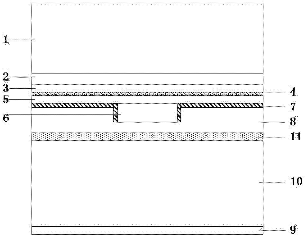
[0041] A flip-chip laser chip based on a SiC substrate, the product structure is as follows Figure 4 shown. include:

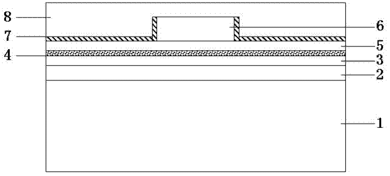
[0042] a. Conventional laser chip, the chip structure includes from bottom to top: GaAs substrate 1, GaAs buffer layer 2, N confinement layer 3, active region 4, P confinement layer 5, GaAs ohmic contact layer 6, SiO 2 Current blocking layer 7, NiAu metal ohmic contact layer 8;

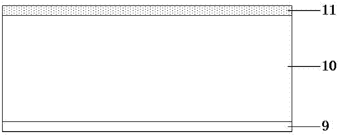
[0043]b. A SiC substrate 10, the bottom surface of the SiC substrate 10 is coated with a NiAu ohmic contact layer 9, and the other side is coated with a TiAu metal bonding layer 11;

[0044] The NiAu metal ohmic contact layer 8 of the conventional laser chip is bonded together through the metal bonding layer 11 on the SiC substrate 10...

Embodiment 2

[0051] For SiC substrate flip-chip lasers, the N electrode is on the top and the P electrode is on the bottom. As described in Example 1, the difference is:

[0052] The conventional laser chip substrate is a GaN substrate, and the laser structure is an oxide strip structure.

[0053] The current blocking layer is selected from SiN 4 The metal bonding layer is selected from Au; the metal ohmic contact layer is selected from CrAu; the electrode metal layer is selected from GeAu.

[0054] The thickness of the metal bonding layer is 3 μm; the thickness of the electrode metal layer is 3 μm.

[0055] A flip-chip laser chip based on a SiC substrate, the product structure includes:

[0056] a. Conventional laser chip, the chip structure includes from bottom to top: GaN substrate, GaN buffer layer, N confinement layer, active region, P confinement layer, GaN ohmic contact layer, SiN 4 Current blocking layer, CrAu metal ohmic contact layer;

[0057] b. A SiC substrate, the bottom ...


PUM

PropertyMeasurementUnit
Thicknessaaaaaaaaaa
Thicknessaaaaaaaaaa
Thicknessaaaaaaaaaa

Abstract

The invention provides an inverted laser chip based on an SiC substrate and a manufacturing method of the inverted laser chip. The inverted laser chip based on the SiC substrate comprises a conventional laser chip structure and the SiC substrate. The conventional laser chip structure sequentially comprises a substrate, a buffer layer, an N limit layer, an active area, a P limit layer, a P-type ohm contact layer, a current retaining layer and a metal ohm contact layer from bottom to top. A metal ohm contact layer is plated at the bottom of the SiC substrate, and a metal bonding layer is plated on the other side. The metal ohm contact layer of the conventional laser chip is bonded with the SiC substrate through the metal bonding layer of the SiC substrate. The N electrode metal layer is evaporated on the buffer layer, with original substrate being removed, of the conventional laser chip. The pole N of the manufactured SiC substrate is at the top, and the pole P of the manufactured SiC substrate is at the bottom. Compared with conventional lasers, the inverted laser chip based on the SiC substrate has the advantages of good radiation, good stability, long service life and the like.

Description

technical field [0001] The invention relates to a flip-chip laser chip based on a SiC substrate and a manufacturing method thereof, belonging to the technical field of laser chips. Background technique [0002] Semiconductor lasers have many advantages such as small size, light weight, high efficiency, long life, easy modulation and low price, and have been widely used in industry, medicine and military fields. Among the various key technologies of semiconductor high-power lasers, the solution to the heat dissipation problem is an extremely critical technology. Because semiconductor lasers can generate high peak power, the electro-optical conversion efficiency of these devices is 40%-50%, that is, 50%-60% of the input electric energy is converted into heat energy. For good heat dissipation, the chip is often soldered to a metal heat sink with high thermal conductivity. Since the thermal expansion coefficients of the laser die and the heat sink are inconsistent, temperature...

Claims


Application Information

Patent Timeline
IPC IPC(8): H01S5/02H01S5/042
Inventor 苏建夏伟张秋霞任忠祥徐现刚
Owner Shandong Huaguang Optoelectronics Co. Ltd.
Why Eureka
Try Eureka