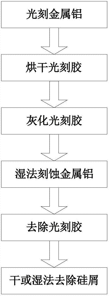
Cleaning method after wet etching
A wet etching and wet removal technology, which is applied in the fields of electrical components, semiconductor/solid-state device manufacturing, circuits, etc., can solve the problem of inability to completely remove silicon shavings, failure to meet product online inspection and shipment inspection requirements, and silicon shavings residue and other issues, to meet the high reliability and high radiation resistance performance, ensure reliability and radiation resistance performance, and reduce the effect of silicon shavings residue
- Summary
- Abstract
- Description
- Claims
- Application Information
AI Technical Summary
Problems solved by technology
Method used
Image


Examples
Embodiment Construction
[0023] In order to make the content of the present invention clearer and easier to understand, the content of the present invention will be further described below in conjunction with the accompanying drawings of the specification. Of course, the present invention is not limited to this specific embodiment, and general replacements well known to those skilled in the art are also covered by the protection scope of the present invention.
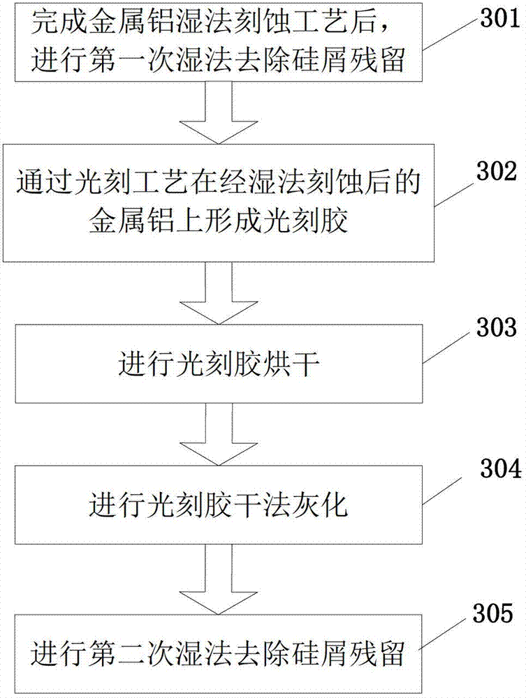
[0024] Refer to below image 3 A preferred embodiment of the cleaning method after wet etching according to the present invention is described.
[0025] Please refer to image 3 , The cleaning method after wet etching of the present invention includes the following steps:
[0026] Step 301: After the metal aluminum wet etching process is completed, perform the first wet removal of silicon residues.
[0027] Among them, the metal aluminum wet etching process is to wet etch the metal aluminum on the thin oxide layer. It should be noted that the thin o...
PUM
| Property | Measurement | Unit |
|---|---|---|
| thickness | aaaaa | aaaaa |
Abstract
Description
Claims
Application Information
 - R&D
- Intellectual Property
- Life Sciences
- Materials
- Tech Scout
- Unparalleled Data Quality
- Higher Quality Content
- 60% Fewer Hallucinations
Browse by: Latest US Patents, China's latest patents, Technical Efficacy Thesaurus, Application Domain, Technology Topic, Popular Technical Reports.
© 2025 PatSnap. All rights reserved.Legal|Privacy policy|Modern Slavery Act Transparency Statement|Sitemap|About US| Contact US: help@patsnap.com