Method for manufacturing fin type field effect transistor and semiconductor structure formed by fin type field effect transistor

一种场效应晶体管、半导体的技术,应用在半导体器件、半导体/固态器件制造、电气元件等方向,能够解决制作高质量的、很难体晶片、FinFET昂贵等问题

Active Publication Date: 2013-04-03
INST OF MICROELECTRONICS CHINESE ACAD OF SCI
View PDF5 Cites 6 Cited by
  • Summary
  • Abstract
  • Description
  • Claims
  • Application Information

AI Technical Summary

Problems solved by technology

However, using SOI wafers to make FinFETs is very expensive
On the other hand, it is difficult to fabricate high-quality FinFETs using conventional bulk wafers due to issues with device width and leakage control below threshold

Method used


Image

  • Method for manufacturing fin type field effect transistor and semiconductor structure formed by fin type field effect transistor
  • Method for manufacturing fin type field effect transistor and semiconductor structure formed by fin type field effect transistor
  • Method for manufacturing fin type field effect transistor and semiconductor structure formed by fin type field effect transistor

Examples


Embodiment Construction

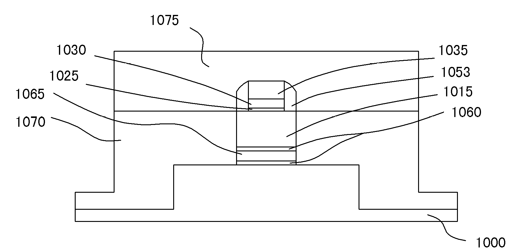
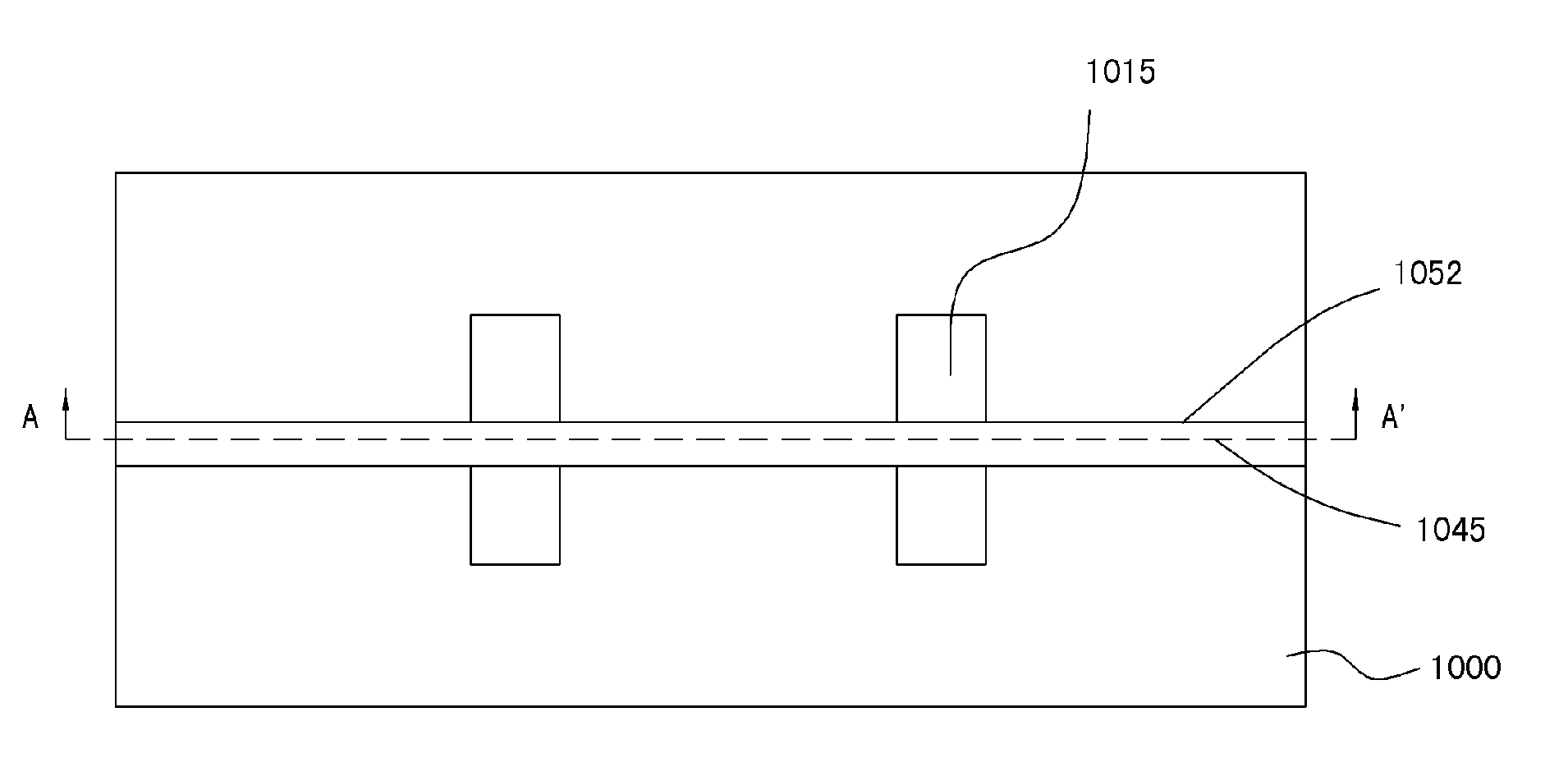
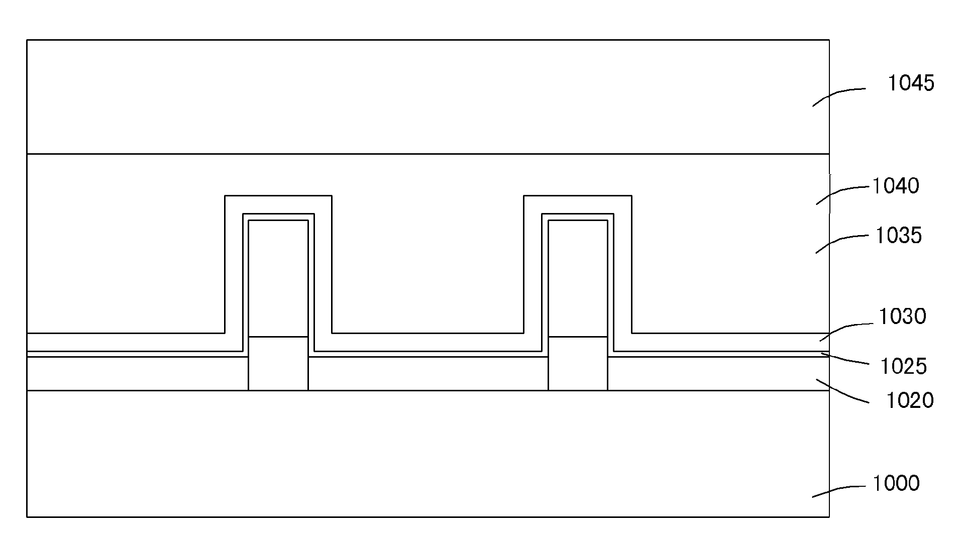
[0012] Hereinafter, the present invention is described by means of specific embodiments shown in the drawings. It should be understood, however, that these descriptions are exemplary only and are not intended to limit the scope of the present invention. Also, in the following description, descriptions of well-known structures and techniques are omitted to avoid unnecessarily obscuring the concept of the present invention.

[0013] A schematic diagram of a layer structure according to an embodiment of the invention is shown in the drawing. The figures are not drawn to scale, with certain details exaggerated and possibly omitted for clarity. The shapes of the various regions and layers shown in the figure, as well as their relative sizes and positional relationships are only exemplary, and may deviate due to manufacturing tolerances or technical limitations in practice, and those skilled in the art will Regions / layers with different shapes, sizes, and relative positions can be...


PUM


Abstract

The invention relates to a method for manufacturing a fin type field effect transistor (FinFET) and a semiconductor structure formed by the fin type field effect transistor. The method for manufacturing the FinFET comprises the following steps of: providing an Si semiconductor substrate, a SiGe layer on the Si semiconductor substrate and a Si layer on the SiGe layer, wherein the SiGe layer is matched with the substrate in a crystal lattice manner; patterning the Si layer and the SiGe layer to form an Fin structure; forming grid stacks on top and two sides of the Fin structure and forming interval side walls surrounding the grid stacks; taking the interval side walls as covering films, removing a part (of the Si layer) on the outer sides of the interval side walls, so as to remain a part (of the Si layer) on the inner sides of the interval side walls; removing a remained part (of the SiGe layer) after patterning to form a gap; forming an insulation substrate in the gap; and externally extending stress source leakage areas, wherein the stress source leakage areas are placed on two sides of the insulation substrate and the Fin structure. The FinFET has good performances (on controlling leakage below a threshold value and width of a component) the same as thoses of an FinFET manufactured by an SOI (silicon on insulator).

Description

technical field [0001] The present invention relates to the field of semiconductors, in particular to a method for manufacturing a FinFET (Fin Field Effect Transistor) and a semiconductor structure formed therefrom. Background technique [0002] As the semiconductor industry advances to the 22nm technology node, some manufacturers have begun to consider how to transition from planar CMOS transistors to three-dimensional (3D) FinFET device structures. Compared with planar transistors, FinFET devices have improved control of the channel, thereby reducing short-channel effects. The gate of the planar transistor is located directly above the channel, while the gate of the FinFET device surrounds the channel on two or three sides, and the channel can be electrostatically controlled from two or three sides. [0003] Currently, there are generally two types of conventional FinFETs: FinFETs formed on silicon-on-insulator (SOI) substrates, and FinFETs formed on bulk Si material subs...

Claims


Application Information

Patent Timeline
Patent Type & Authority Applications(China)
IPC IPC(8): H01L21/336H01L29/78
CPCH01L29/66795H01L29/7851H01L29/7848H01L29/7856
Inventor 朱慧珑骆志炯尹海洲
Owner INST OF MICROELECTRONICS CHINESE ACAD OF SCI
Why Eureka
Try Eureka