Magnetron sputtering apparatus and method

A magnetron sputtering device and magnetron sputtering technology, applied in the direction of sputtering plating, ion implantation plating, coating, etc., can solve the problem of difficult high-speed film formation, reduced film formation efficiency, large recoil Ar energy, etc. problems, to achieve the effect of ensuring in-plane uniformity, improving film forming efficiency, and ensuring film forming speed

Inactive Publication Date: 2013-04-10
TOKYO ELECTRON LTD
View PDF4 Cites 7 Cited by
  • Summary
  • Abstract
  • Description
  • Claims
  • Application Information

AI Technical Summary

Problems solved by technology

The sputtered threshold voltage of W is about 33eV, and it is clear that the recoil energy of Ar is greater than this value, which causes a large number of defects to be generated in the film.
In addition, the amount of Ar in the film also increases, which causes the increase in resistance together with defects.
However, in the conventional magnetron sputtering apparatus, since the distance between the target and the substrate is long and the plasma density near the substrate is low by causing discharge in a low-pressure environment, it is necessary to energize Ar ions with high energy.
Therefore, it is necessary to apply a high-potential high-frequency power to the substrate, but as a result, since a negative potential more than necessary is generated on the substrate, Ar ions with excess energy are drawn onto the substrate, and the Ar ions protrude into the substrate as described above. The W film obtained by film formation causes defects on the film
It is conceivable to increase the pressure in order to reduce the applied high-frequency power, but as described above, the film formation efficiency becomes lower
[0024] As mentioned above, in the conventional magnetron sputtering apparatus in which the distance between the target 13 and the substrate is 50 mm to 100 mm, in the case of forming a film of a high-melting point metal such as W, it is currently difficult to satisfy both high-speed film formation and formation. Conditions for membrane efficiency, target usage efficiency, low electrical resistance and good membrane quality

Method used


Image

  • Magnetron sputtering apparatus and method
  • Magnetron sputtering apparatus and method
  • Magnetron sputtering apparatus and method

Examples


Embodiment 1)

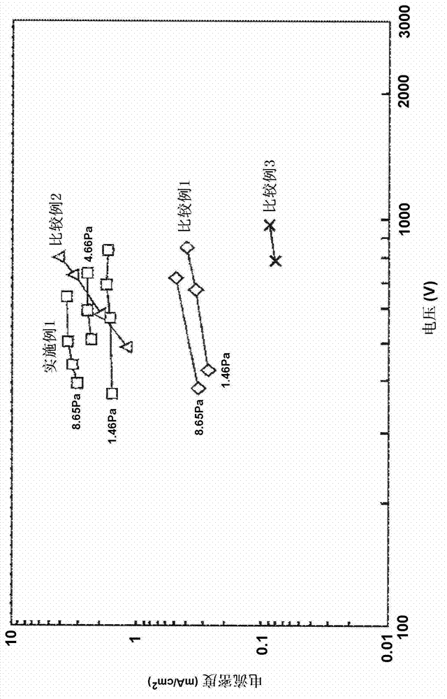
[0228] in having Figure 11 In the magnetron sputtering apparatus for the magnet array body 511, the film formation process was performed under the above-mentioned process conditions, and the relationship between the DC voltage applied to the target electrode 3 and the power density was evaluated. At this time, the distance between the target 31 and the wafer 10 was set to 30 mm. In addition, for the configuration in which the return magnet 531 is not provided in the magnet array body 511 (comparative example 1), Figure 23 The configuration (comparative example 2) using the conventional magnetron sputtering apparatus shown above and the configuration (comparative example 3) that discharges by applying a DC voltage without using a magnet were also evaluated in the same manner.

[0229] Figure 16 Indicates the result. In the figure, the horizontal axis represents the DC voltage applied to the target electrode 3, and the vertical axis represents the current density between t...

Embodiment 2)

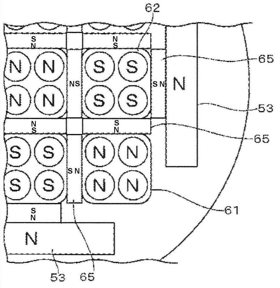
[0232] in having figure 2 In the magnetron sputtering apparatus of the magnet array body 5, without rotating the magnet array body 5, the film-forming process was performed under the above-mentioned processing conditions, and the film-forming speed distribution in the wafer diameter direction was obtained. Also, for instead of figure 2 The magnet array body 5 is provided with Figure 10 In the case of the magnet array body 5A, the film formation rate was also measured in the same manner. For this result, Figure 17 Indicates the configuration in which the magnet array body 5 is provided, Figure 18 A configuration in which the magnet array body 5A is provided is shown.

[0233] Here, the difference between the magnet array body 5 and the magnet array body 5A is only the number of magnet units 63 constituting the magnets 61, 62, but it has been confirmed that by adjusting the number of magnet units 63, the radial direction of the wafer 10 can be changed. film-forming vel...

Embodiment 3)

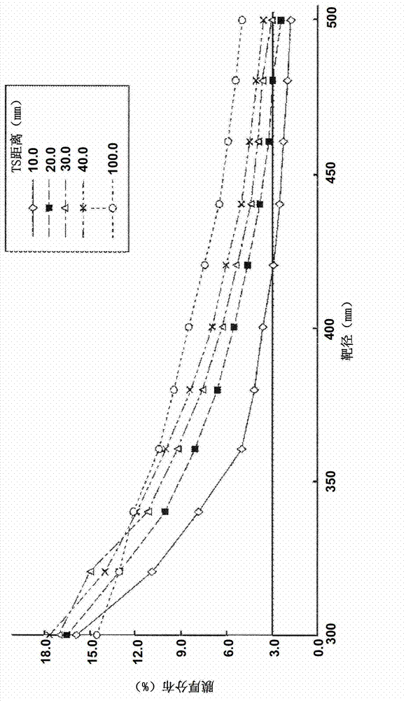
[0237] in having figure 2 In the magnetron sputtering of the magnet array body 5, the distance between the target 31 and the wafer 10 is set to 20mm, and the magnet array body 5 is not rotated, and the film formation process is performed under the above-mentioned processing conditions, and the Film formation velocity distribution in the radial direction of the wafer. In addition, the film formation rate was measured similarly also about the case where the distance between the target 31 and the wafer 10 was set to 50 mm. This result is shown together with the arrangement of the magnet group 5 of the magnet arrangement body 5 and the corrosion of the target 31 in Figure 19 . In addition, in this Example 3, the target 31 larger than the magnet group 52 of the magnet array body 5 was used.

[0238] From this, it can be confirmed that when the distance between the target 31 and the wafer 10 is 20 mm, the in-plane uniformity of the film formation rate is higher than when the di...


PUM

PropertyMeasurementUnit
electrical resistivityaaaaaaaaaa
diameteraaaaaaaaaa

Abstract

A magnetron sputtering apparatus in which a target is disposed to face a substrate includes a magnet array body including a magnet group arranged on a base body, and a rotating mechanism for rotating the magnet array body around an axis perpendicular to the substrate. In the magnet array body, N poles and S poles constituting the magnet group are arranged to be spaced from each other along a surface facing the target such that a plasma is generated based on a drift of electrons by a cusp magnetic field. Magnets located on the outermost periphery of the magnet group are arranged in a line to prevent the electrons from being released from constraint of the cusp magnetic field and jumping out of the cusp magnetic field. A distance between the target and the substrate during sputtering is equal to or less than 30 mm.

Description

[0001] technology area [0002] The invention relates to a magnetron sputtering device and a magnetron sputtering method. Background technique [0003] Magnetron sputtering devices used in the manufacturing process of semiconductor devices, such as Figure 33 The configuration shown is such that a target 13 made of a film-forming material is arranged to face a substrate (substrate) 12 in a vacuum container 11 set to a low-pressure atmosphere, and a target 13 is provided on the upper surface side of the target 13. When the target 13 is a conductor such as metal, the magnet 14 forms a magnetic field near the lower surface of the target 13 in a state where a negative DC voltage is applied. In addition, in order to prevent particles from adhering to the inner wall of the vacuum container 11 , an anti-adhesion shield (not shown) is provided. [0004] The above-mentioned magnet 14, such as Figure 34 As shown, in general, for example, a circular magnet 16 having a polarity differe...

Claims


Application Information

Patent Timeline
Patent Type & Authority Applications(China)
IPC IPC(8): C23C14/35
CPCC23C14/35H01J37/32688H01J37/3405H01J37/3452H01J37/3455H01L21/203
Inventor 水野茂户岛宏至五味淳宫下哲也波多野达夫水泽宁
Owner TOKYO ELECTRON LTD
Why Eureka
Try Eureka