
Method for preparing intermediate and long infrared undercut type optical waveguides based on silicon on insulator (SOI) materials

A long-infrared and optical waveguide technology, applied in light guides, optics, optical components, etc., can solve the problems of mode leakage, high silicon dioxide loss, and limited light field, etc., and achieve low transmission loss, easy purchase, and flexible design.

Inactive Publication Date: 2013-04-10
ZHEJIANG UNIV
View PDF1 Cites 13 Cited by
  • Summary
  • Abstract
  • Description
  • Claims
  • Application Information

AI Technical Summary

Problems solved by technology

In the entire medium and long infrared band (except 2.9-3.6μm), the loss of silica is very high
Therefore, when the wavelength is greater than 3.6 μm, the SOI waveguide buried oxide layer will introduce a large absorption loss
At the same time, in the mid-to-long infrared band, the oxide layer as a confinement layer in the near-infrared band cannot confine the light field very well, and mode leakage will occur, which will also introduce a large transmission loss.

Method used


Image

  • Method for preparing intermediate and long infrared undercut type optical waveguides based on silicon on insulator (SOI) materials
  • Method for preparing intermediate and long infrared undercut type optical waveguides based on silicon on insulator (SOI) materials
  • Method for preparing intermediate and long infrared undercut type optical waveguides based on silicon on insulator (SOI) materials

Examples


Embodiment Construction

[0028] The present invention will be further described below in conjunction with the accompanying drawings and embodiments.

[0029] 1. Cleavage the SOI sheet into the desired size, clean and dry according to the standard cleaning process, and clean the photolithography plate at the same time;

[0030] 2. Put the SOI sheet into the thermal oxidation furnace, alternately perform dry oxygen and wet oxygen twice, so that it grows a dense oxide layer with a thickness of about 600nm;

[0031] 3. Spin-coat the photoresist with a coating machine and pre-bake it for 30 minutes, then use a photolithography machine to transfer the waveguide pattern on the photoresist board to the SOI sheet, develop, shape, post-bake, and harden the film;

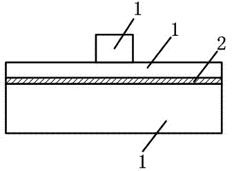
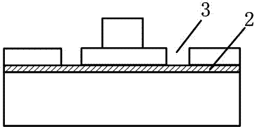
[0032] 4. Etch the waveguide on the upper surface silicon 1 by dry etching or wet etching process, such as figure 1 , figure 2 shown;

[0033] 5. Clean the SOI sheet again, put it into a thermal oxidation furnace for secondary oxidation to prepare...


PUM


Abstract

The invention discloses a method for preparing intermediate and long infrared undercut type optical waveguides based on silicon on insulator (SOI) materials. A row of square holes are formed in two sides of a ridge waveguide on an SOI piece, parallel to the ridge waveguide, and distributed at intervals. A high-loss oxygen buried layer under the ridge waveguide is hollowed out through the square holes so that an intermediate and long infrared undercut type ridge waveguide structure is achieved. Or slots are etched at the center of the ridge waveguide on the SOI piece, and a high-loss oxygen buried layer under the slot type waveguide is hollowed out trough the slots so that an intermediate and long infrared undercut type slot waveguide structure is achieved. Two manufactured waveguide structures through the method have low transmission loss, and a light field of the undercut type slot waveguide is mainly limited in the slots with a low refractive index. If chemical materials which can absorb existing characteristics of intermediate and long infrared bands are filled in the slots, an intermediate and long infrared absorption type sensor can be formed.

Description

technical field [0001] The invention relates to a method for preparing a medium-long infrared low-loss optical waveguide, in particular to a method for preparing a medium-long infrared undercut optical waveguide based on an SOI material. Background technique [0002] Since the new century, the IT industry represented by the Internet and the new generation of mobile communication technology has greatly promoted the research and development of integrated optoelectronic devices, and its own development has also promoted their application scope, gradually expanding from the communication field to the industrial , military, energy, medical, biological, sensing and other fields. In particular, silicon-based optoelectronic devices combined with the current mature CMOS technology create the possibility of low-cost, large-scale functionalization and modularization. [0003] So far, the research on integrated optics has mainly focused on the near-infrared band, mainly at 1.55 μm. How...

Claims


Application Information

Patent Timeline
Patent Type & Authority Applications(China)
IPC IPC(8): G02B6/136
Inventor 檀亚松余辉郝寅雷李宇波杨建义江晓清
Owner ZHEJIANG UNIV
Learn More