
Schottky diode

A technology of Schottky diodes and diodes, applied in the direction of electrical components, electric solid devices, circuits, etc., can solve the problems of inconvenient use, not displaying the working parameters of Schottky diodes, etc., and achieve the effect of convenient and correct use and simple structure

Inactive Publication Date: 2013-04-10
孔明
View PDF0 Cites 2 Cited by
  • Summary
  • Abstract
  • Description
  • Claims
  • Application Information

AI Technical Summary

Problems solved by technology

Most of the medium and low power Schottky diodes are packaged, but the working parameters of the Schottky diode are not displayed on the package, which is inconvenient to use

Method used


Image

  • Schottky diode
  • Schottky diode

Examples


Embodiment Construction

[0011] The present invention will now be further described in conjunction with specific examples, and the following examples are intended to illustrate the present invention rather than further limit the present invention.

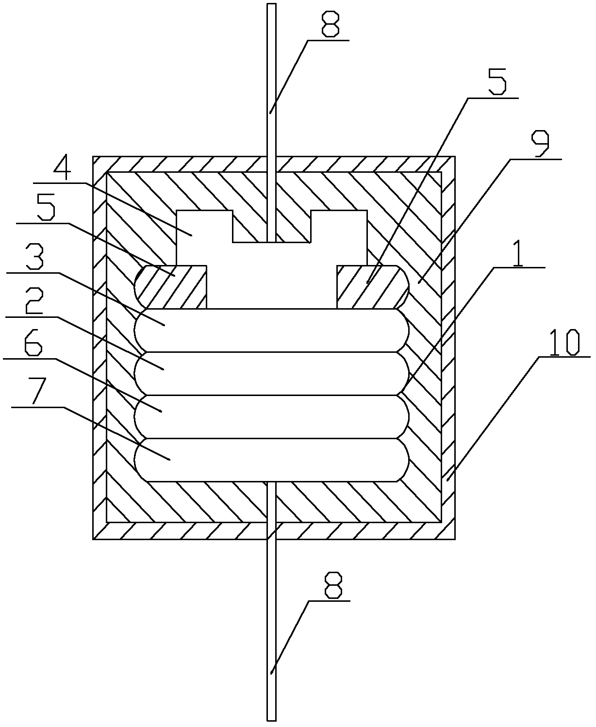
[0012] Such as Figure 1~2 The Schottky diode shown includes a diode body 1, the diode body 1 uses an N-type semiconductor as a substrate 2, and an N-epitaxial layer 3 using arsenic as a dopant is formed on the substrate 2, and on the N-epitaxial layer 3 There is an anode metal 4 in contact with it, and the edge region of the anode metal 4 is provided with a silicon dioxide layer 5, and an N+ cathode layer 6 is formed under the substrate 2, and there is a cathode metal 7 in contact with it under the N+ cathode layer 6, and the anode metal 4 An electrode 8 is drawn out from the cathode metal 7, and the diode body 1 is plastic-sealed in an epoxy resin tube 9, and the epoxy resin tube 9 is coated with a layer of coating 10 that can clearly display the working...


PUM


Abstract

The invention relates to a semiconductor element, in particular to a schottky diode. The schottky diode comprises a diode body. The diode body is provided with a chip made of N-type semiconductor, an N- epitaxial layer using arsenic as dopant is covered on the chip, an anodic metal contacting with the N- epitaxial layer is arranged on the N-epitaxial layer, and a silica layer is arranged at the edge area of the anodic metal. An N+ cathode layer is arranged under the chip, a cathode metal contacting with the N+ cathode layer is arranged under the N+ cathode layer, and both the anodic metal and the cathode metal are respectively connected with an electrode. The diode body is sealed in an epoxy resin tube with plastic, and a coating layer which can display the working parameters of the diode body clearly is coated outside the epoxy resin tube. The schottky diode has the advantages that the structure is simple, the electrical specification of the diode body is unaffected by sealing the diode body in the epoxy resin tube with plastic, the coating layer coated outside the epoxy resin can display the working parameters of the diode body clearly, and the schottky diode is convenient to use correctly.

Description

technical field [0001] The invention relates to a semiconductor device, especially a Schottky diode. Background technique [0002] Schottky diodes are not made using the principle of a P-type semiconductor contacting an N-type semiconductor to form a PN junction, but using the principle of a metal-semiconductor junction formed by contacting a metal and a semiconductor. Therefore, Schottky diodes are also called metal-semiconductor (contact) diodes or surface barrier diodes, which are a type of hot-carrier diode. Schottky diodes are low-power, high-current, ultra-high-speed semiconductor devices that have come out in recent years. Its reverse recovery time is extremely short (can be as small as a few nanoseconds), the forward voltage drop is only about 0.4V, and the rectification current can reach several thousand mA. These excellent characteristics are unmatched by fast recovery diodes. Most of the medium and low-power Schottky diodes are packaged, but the working paramete...

Claims


Application Information

Patent Timeline
Patent Type & Authority Applications(China)
IPC IPC(8): H01L23/29
CPCH01L24/01H01L2924/12032
Inventor 孔明
Owner 孔明
Learn More