Semiconductor device and manufacturing method of the same

A manufacturing method and semiconductor technology, which is applied in semiconductor/solid-state device manufacturing, semiconductor devices, semiconductor/solid-state device components, etc., can solve problems such as increased resistance and decreased yield, and achieve the effect of increased yield

Active Publication Date: 2013-04-10
SONY CORP
View PDF2 Cites 10 Cited by
  • Summary
  • Abstract
  • Description
  • Claims
  • Application Information

AI Technical Summary

Problems solved by technology

The metal-based deposits are not removed after ashing or chemical post-treatment, resulting in particle generation and reduced yield
Also, this overetching of the shallow conductive material layer can cause complete penetration of the conductive material layer
In this case, when the final metal is filled into the connection hole, the metal may only come into contact with the sides of the conductive material layer, thus resulting in increased resistance

Method used


Image

  • Semiconductor device and manufacturing method of the same
  • Semiconductor device and manufacturing method of the same
  • Semiconductor device and manufacturing method of the same

Examples


no. 1 approach

[0021] 1. First Embodiment (Structure of Semiconductor Device)

[0022] 2. First Embodiment (Manufacturing method in which the first wiring exposed at the bottom of the previously formed large-diameter recess is covered with a small-diameter resist pattern)

[0023] 3. Second embodiment (manufacturing method in which etching is stopped midway so that the unetched thicknesses above the first wiring and the second wiring are uniform)

[0024] 4. Third Embodiment (Manufacturing Method Using Interlayer Insulator Film as Etching Stopper to Stop Etching Halfway)

[0025] 5. Fourth Embodiment (Manufacturing Method of Filling a Filling Member into a Concavity Formed by Stopping Etching Halfway)

no. 5 approach

[0026] 6. Fifth Embodiment (Manufacturing Method of Remaining Resist Material for Covering Second Wiring in Previously Formed Small-diameter Recess)

[0027] 7. Sixth embodiment (manufacturing method in which etching is stopped midway so that the unetched thicknesses above the first wiring and the second wiring are uniform)

[0028] 8. Seventh Embodiment (Manufacturing method in which etching is stopped halfway to make unetched thicknesses above first wiring and second wiring uniform and a hard mask is used)

[0029] It should be noted that similar components in the respective embodiments and modifications are denoted by the same reference numerals, and repeated descriptions are omitted.

[0030]

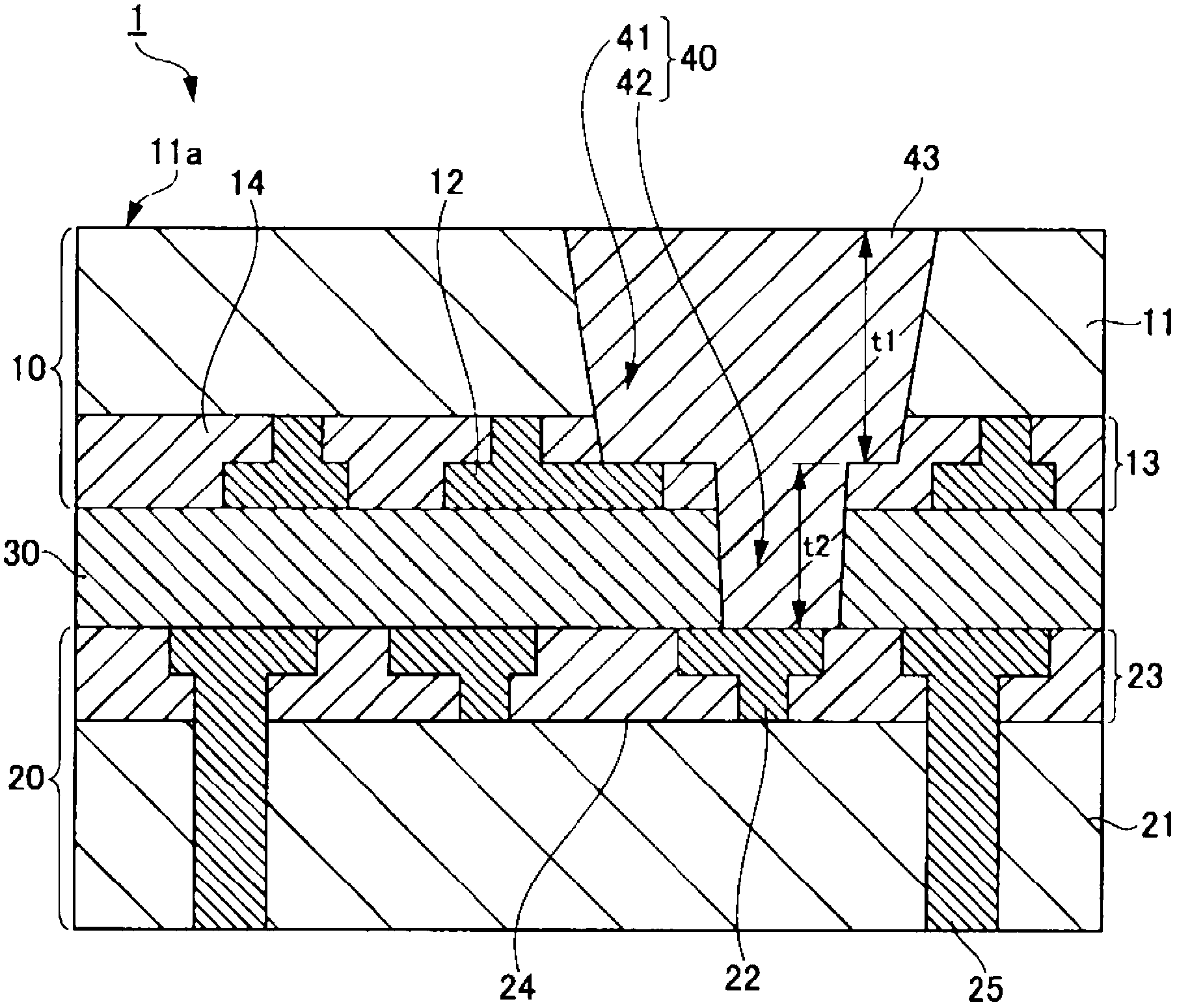
[0031] figure 1 is a cross-sectional view of main components of the semiconductor device of the first embodiment. Next, the semiconductor device of the first embodiment will be described in detail based on the cross-sectional view of the main components.

[0032] figure 1 The ...

Embodiment approach

[0053]

[0054] Below, refer to Figure 2A ~ Figure 2G The cross-sectional step diagrams shown illustrate the method of manufacturing the semiconductor device 1 of the first embodiment described above.

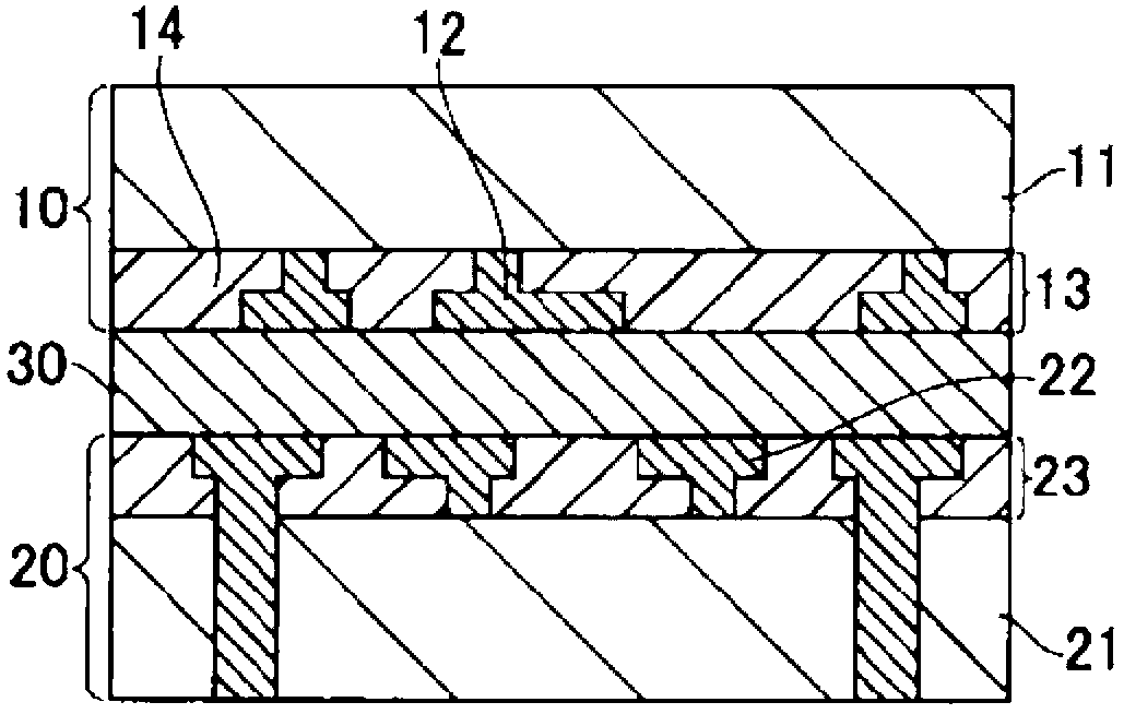
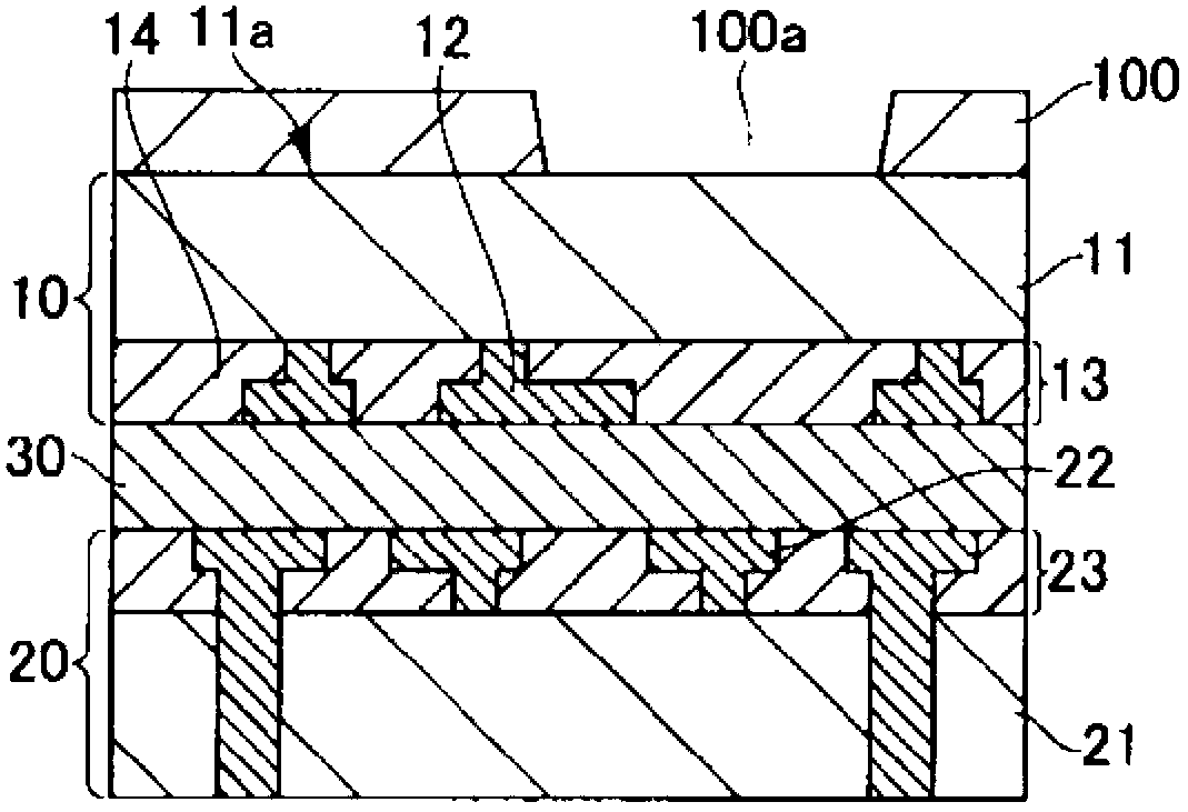
[0055] Such as Figure 2A As shown, a first substrate 10 and a second substrate 20 are manufactured. The wiring layer 13 including the first wiring 12 is provided on one main surface side of the semiconductor layer 11 of the first substrate 10 . The wiring layer 23 including the second wiring 22 is provided on one main surface side of the semiconductor layer 21 of the second substrate 20 . The first substrate 10 and the second substrate 20 are bonded together through the bonding portion 30 interposed between the wiring layer 13 and the wiring layer 23, and thus a bonded substrate is manufactured.

[0056] It should be noted that the steps up to this point are not specifically limited, and the steps can be carried out using usual techniques. The step of forming connection...


PUM


Abstract

Disclosed herein is a semiconductor device including: a substrate having a first conductive layer and a second conductive layer arranged deeper than the first conductive layer; a large-diameter concave portion having, on a main side of a substrate, an opening sized to overlap the first and second conductive layers, with the first conductive layer exposed in part of the bottom of the large-diameter concave portion; a small-diameter concave portion extended from the large-diameter concave portion and formed by digging into the bottom of the large-diameter concave portion, with the second conductive layer exposed at the bottom of the small-diameter concave portion; and a conductive member provided in a connection hole made up of the large- and small-diameter concave portions to connect the first and second conductive layers.

Description

[0001] Cross References to Related Applications [0002] This application contains subject matter related to and claims priority from Japanese Patent Application JP2011-219843 filed in Japan Patent Office on Oct. 4, 2011, the entire content of which is hereby incorporated by reference. technical field [0003] The present invention relates to a semiconductor device in which conductive layers at different heights are exposed in connection holes and a manufacturing method thereof. Background technique [0004] LSI and other semiconductor devices have achieved miniaturization and high performance due to high-density integration due to microfabrication processes. In such high-density integrated semiconductor devices, new ideas have been proposed to reduce the necessary area of ​​the interlayer connection structure of multilayer wiring. For example, Japanese Patent Laid-Open No. 1997-199586 discloses a semiconductor device having a common contact structure. In this semiconducto...

Claims


Application Information

Patent Timeline
Patent Type & Authority Applications(China)
IPC IPC(8): H01L23/528H01L21/768
CPCH01L23/481H01L21/76898H01L25/50H01L2225/06541H01L2924/0002H01L27/14636H01L25/0657H01L24/32H01L2224/32145H01L23/5226H01L23/528H01L2924/00
Inventor 深沢正永
Owner SONY CORP
Why Eureka
Try Eureka