Compound semiconductor device and method for fabricating the same
A semiconductor and compound technology, applied in the fields of semiconductor/solid-state device manufacturing, semiconductor devices, semiconductor/solid-state device components, etc., can solve the problems of the most difficult p-type GaN structure, the GaN manufacturing technology is not as developed and optimized as the Si manufacturing technology, etc.
- Summary
- Abstract
- Description
- Claims
- Application Information
AI Technical Summary
Problems solved by technology
Method used
Image

Examples
no. 1 approach
[0034] In the first embodiment, an AlGaN / GaN HEMT as a compound semiconductor device is disclosed.
[0035] 1 and 3 are schematic cross-sectional views showing step by step a method for manufacturing an AlGaN / GaN HEMT according to a first embodiment.
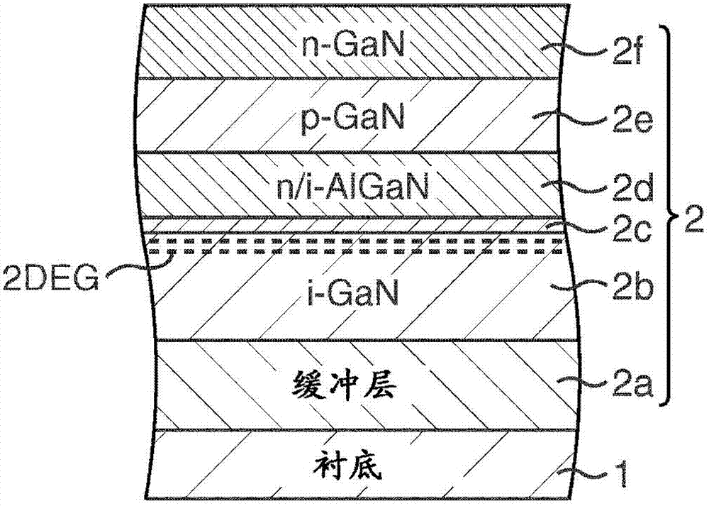
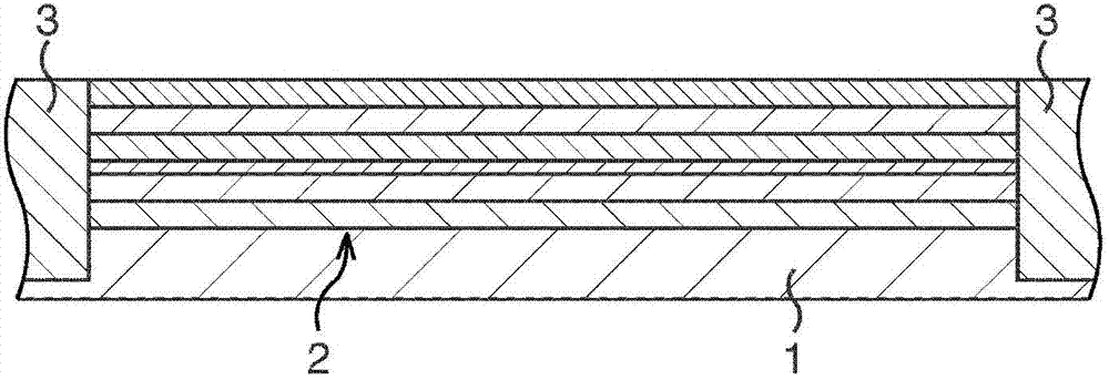
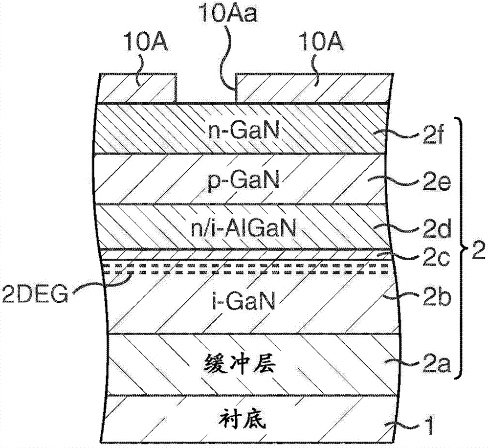
[0036] Such as Figure 1A As shown, firstly, a compound semiconductor multilayer structure 2 is formed on a growth substrate (for example, a Si substrate 1). The growth substrate can also be other materials such as sapphire substrate, GaAs substrate, SiC substrate or GaN substrate instead of Si substrate. The substrate may be a semi-insulating substrate or a conductive substrate.
[0037] The compound semiconductor multilayer structure 2 includes a buffer layer 2a, an electron transport layer 2b, an intermediate layer (spacer layer) 2c, an electron supply layer 2d, a p-type cladding layer 2e, and an n-type cladding layer 2f. Here, as will be described later, the electron transport layer 2b has negative polarity so that a two-...
no. 2 approach
[0091] In the second embodiment, an AlGaN / GaN high electron mobility diode (hereinafter, simply referred to as an AlGaN / GaN diode) will be disclosed as a compound semiconductor device.
[0092] 10 to 12 are schematic cross-sectional views showing step by step a method for manufacturing the AlGaN / GaN diode according to the second embodiment.
[0093] Such as Figure 10A As shown, first, a compound semiconductor multilayer structure 21 is formed on a growth substrate (for example, Si substrate 1). The growth substrate can be other materials such as sapphire substrate, GaAs substrate, SiC substrate or GaN substrate. The substrate may be a semi-insulating substrate or a conductive substrate.
[0094] The compound semiconductor multilayer structure 21 includes a buffer layer 21a, an electron transport layer 21b, an intermediate layer (spacer layer) 21c, an electron supply layer 21d, a p-type cladding layer 21e, and an n-type cladding layer 21f.
[0095] Specifically, the followi...
no. 3 approach
[0138] In a third embodiment, a power factor correction (PFC) circuit comprising an AlGaN / GaN HEMT according to the first embodiment and / or an AlGaN / GaN according to the second embodiment will be disclosed.
[0139] Figure 17 is the connection diagram of the PFC circuit.
[0140] The PFC circuit 30 includes a switching element (transistor) 31 , a diode 32 , a choke coil 33 , capacitors 34 , 35 , a diode bridge 36 , and an alternating current power supply (AC) 37 . The AlGaN / GaN HEMT according to the first embodiment is applied to the switching element 31 . Alternatively, the AlGaN / GaN diode according to the second embodiment is applied to the diode 32 . Alternatively, an AlGaN / GaN HEMT according to the first embodiment is applied to the switching element 31 and an AlGaN / GaN diode according to the second embodiment is applied to the diode 32 . The AlGaN / GaN diode according to the second embodiment can also be applied to the diode bridge 36 .
[0141] In the PFC circuit 30,...
PUM
 Abstract
Description
Claims
Application Information
 - R&D
- Intellectual Property
- Life Sciences
- Materials
- Tech Scout
- Unparalleled Data Quality
- Higher Quality Content
- 60% Fewer Hallucinations
Browse by: Latest US Patents, China's latest patents, Technical Efficacy Thesaurus, Application Domain, Technology Topic, Popular Technical Reports.
© 2025 PatSnap. All rights reserved.Legal|Privacy policy|Modern Slavery Act Transparency Statement|Sitemap|About US| Contact US: help@patsnap.com