High-voltage transistor model method with expandable drift region resistor

A technology of high-voltage transistors and drift regions, applied in electrical digital data processing, special data processing applications, instruments, etc.

Inactive Publication Date: 2013-04-17
SHANGHAI HUAHONG GRACE SEMICON MFG CORP
View PDF2 Cites 7 Cited by
  • Summary
  • Abstract
  • Description
  • Claims
  • Application Information

AI Technical Summary

Problems solved by technology

[0004] However, the field plate technology will also introduce a large overlap capacitance (Overlap capacitance), and the large re

Method used


Image

  • High-voltage transistor model method with expandable drift region resistor
  • High-voltage transistor model method with expandable drift region resistor
  • High-voltage transistor model method with expandable drift region resistor

Examples


Embodiment Construction

[0066] The present invention has the high-voltage transistor model method of extensible drift region resistance, comprises the following steps:

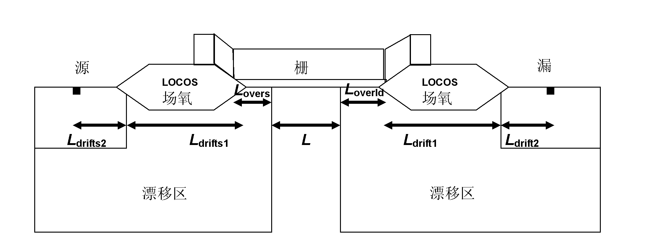
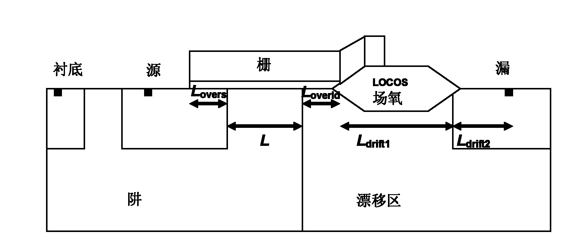
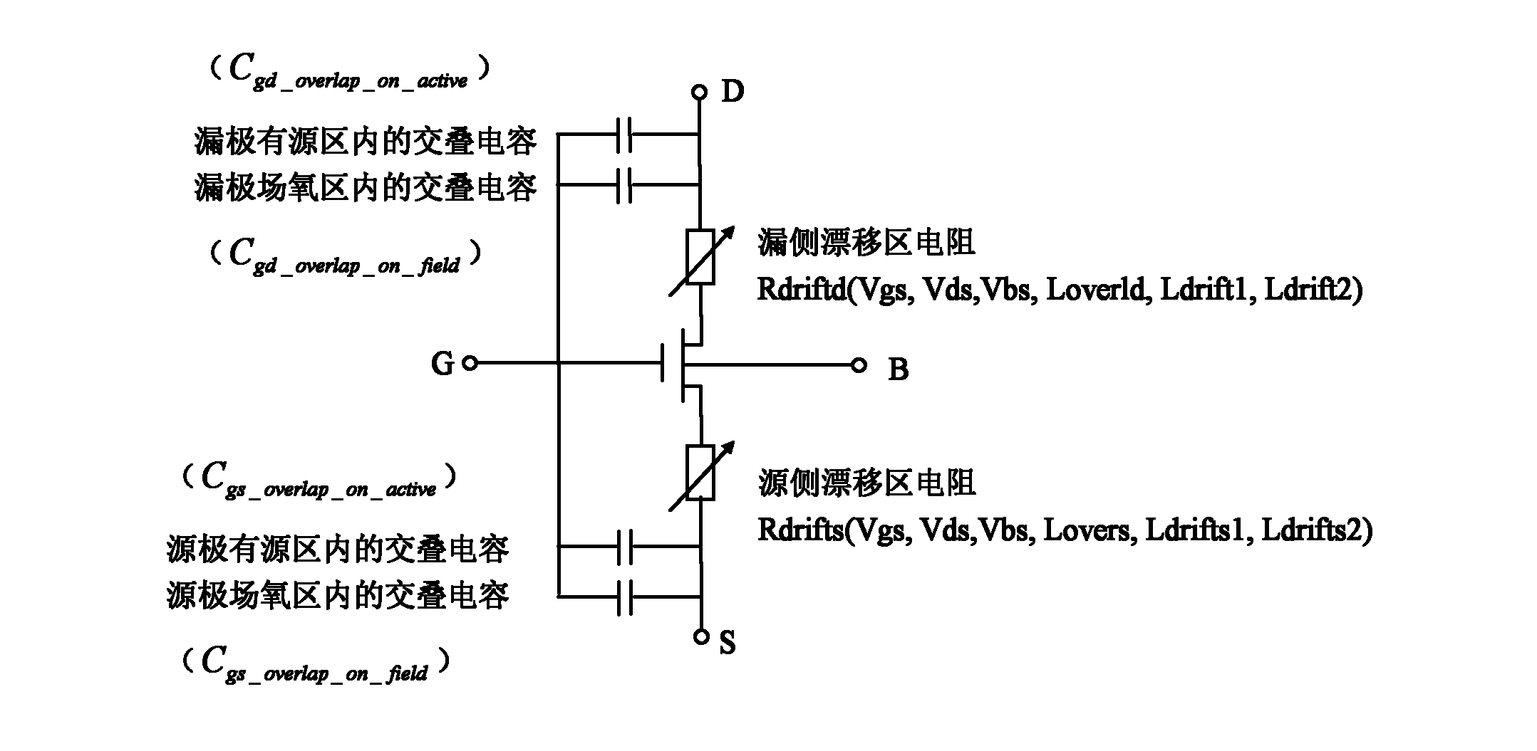
[0067] first step, such as figure 1 , figure 2 As shown, according to the device structure, the drain side drift region is divided into three parts: the drift region Loverld under the channel active region, the drift region Ldrift1 under the field oxygen region, and the drift region Ldrift2 under the drain active region; the source side drift region The area is also divided into three parts: the drift area Lovers under the channel active area, the drift area Ldrifts1 under the field oxygen, and the drift area Ldrifts2 under the source active area;

[0068] in:

[0069] L is the device channel length;

[0070] Loverld is the length of the drain side drift region in the active region of the channel;

[0071] Ldrift1 is the length of the drift region on the drain side under field oxygen;

[0072] Ldrift2 is the length of the drain...


PUM


Abstract

The invention discloses a high-voltage transistor model method with an expandable drift region resistor. The method includes the following steps: step 1, a drain-side drift region is divided into three portions according to a device structure, and the three portions include a drift region Lover1d under a ditch active area, a drift region Ldrift1 under filed oxygen and a drift region Ldrift2 under a drain active area; and a source-side drift region is also divided into three portions: a drift region Lovers under the ditch active area, a drift region Ldrifts1 under the field oxygen and a drift region Ldrifts2 under a source active area; and step 2, a resistor property of drift regions of each portion is simultaneously simulated, and effects of gate source voltage Vgs, drain source voltage Vds and body source voltage Vbs of a device on the drift region resistor property are simulated through the following formula. By means of the high-voltage transistor model method, precision of a high-voltage metal oxide semiconductor (MOS) model or a high-voltage laterally diffused metal oxide semiconductor (LDMOS) model can be effectively improved, simulation precision of a high-voltage integrated circuit is improved, and a circuit design period is shortened.

Description

technical field [0001] The invention relates to a high-voltage transistor model method, in particular to a high-voltage transistor model method with scalable drift region resistance. Background technique [0002] High-voltage transistors used in high-voltage integrated circuit design are generally divided into high-voltage MOS and high-voltage LDMOS. There are currently two methods for improving the withstand voltage of high-voltage transistors: first, the introduction of field plate technology can uniform the surface electric field, thereby increasing the breakdown voltage of the device; second, on the withstand voltage side (drain side or both sides of the source and drain) A lightly doped drift region is introduced, and the breakdown voltage of the device is increased through the depletion of the drift region. [0003] Such as figure 1 As shown, in order to improve the breakdown voltage of the device, a lightly doped drift region is introduced on the source side and the...

Claims


Application Information

Patent Timeline
IPC IPC(8): G06F17/50
Inventor 武洁
Owner SHANGHAI HUAHONG GRACE SEMICON MFG CORP
Why Eureka
Try Eureka