Method for making circuit structure

A technology of circuit structure and production method, applied in the direction of printed circuit manufacturing, printed circuit, electrical components, etc., can solve the problems of long electroplating time material cost and time cost, prolong electroplating time, increase production cost, etc., so as to avoid production cost The waste of time and cost, the effect of avoiding environmental pollution

Inactive Publication Date: 2013-04-17
UNIMICRON TECH CORP
View PDF4 Cites 6 Cited by
  • Summary
  • Abstract
  • Description
  • Claims
  • Application Information

AI Technical Summary

Problems solved by technology

Therefore, the material cost and time cost of longer electroplating time to form a thicker conductive copper layer, the material cost and time cost of removing the conductive copper layer on the surface of the dielectric layer, and the excessive and unnecessary The production cost and time cost of the by-products and waste derived from the production conditions are a waste
Furthermore, the conductive copper layer increased by prolonging the electroplating time may also have uneven thickness distribution, which will not be conducive to the subsequent production of build-up circuit layers on it, let alone the production of stacked hole design or higher wiring. The problem of low production process yield of density circuit board and low reliability circuit structure
In addition, if photolithography and etching are used to form the circuit structure, it will face problems such as the use of a large amount of chemical liquid, which will cause environmental pollution and increase production costs.

Method used


Image

  • Method for making circuit structure
  • Method for making circuit structure
  • Method for making circuit structure

Examples


Embodiment Construction

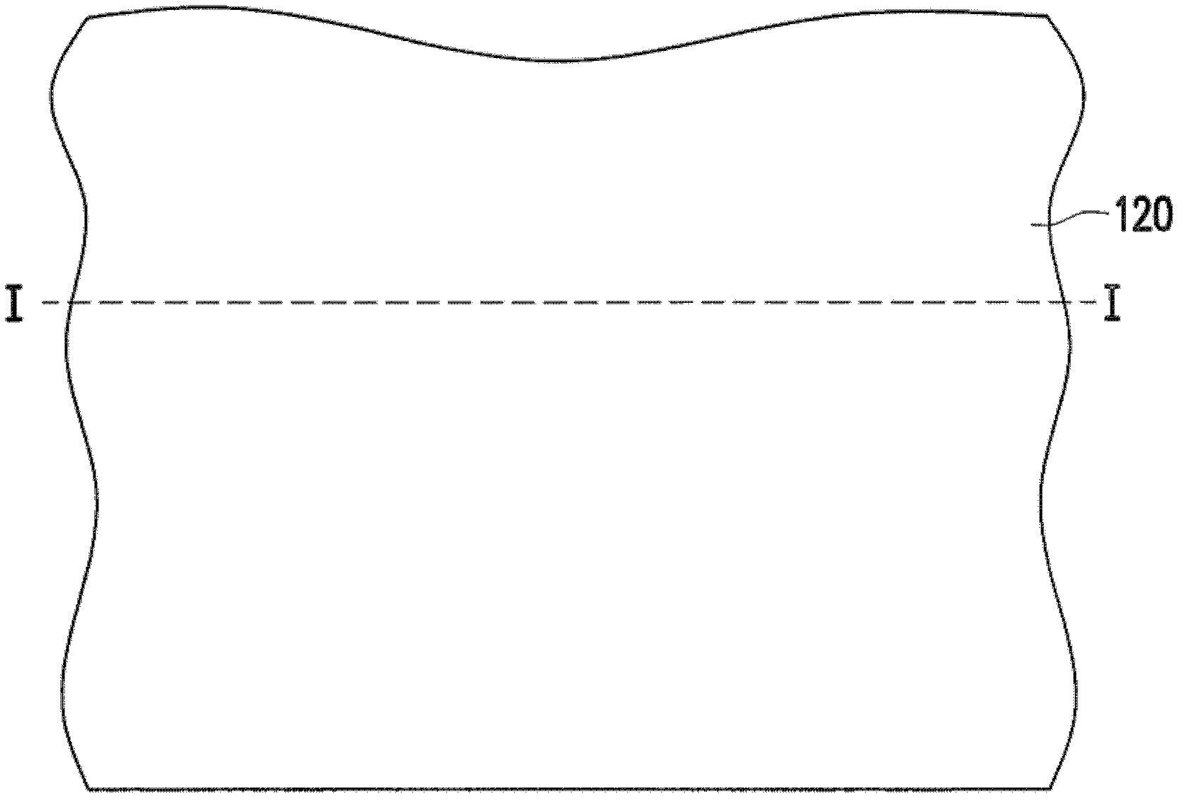
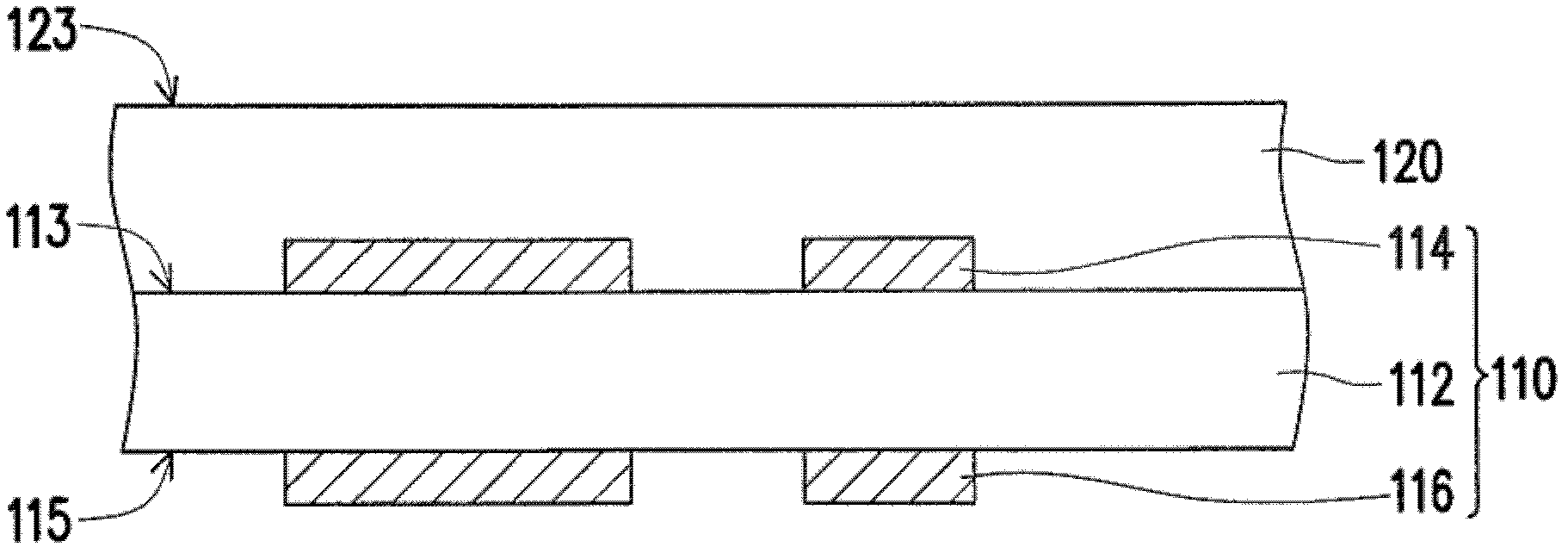
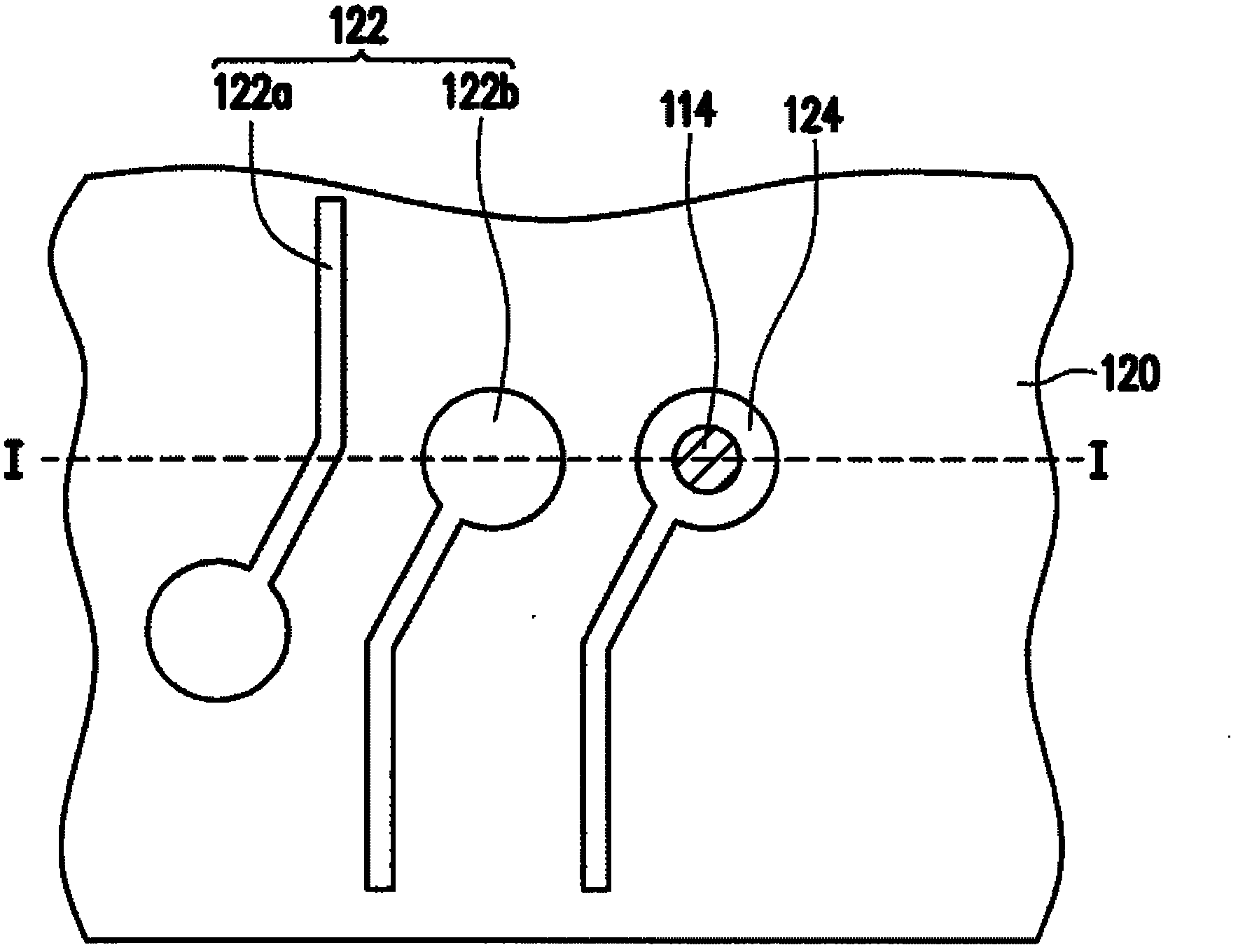
[0033] Figure 1A to Figure 1G It is a schematic top view of a manufacturing method of a circuit structure according to an embodiment of the present invention. Figure 2A to Figure 2G respectively draw along Figure 1A to Figure 1G Schematic cross-section of the line I-I. Please also refer to Figure 1A and Figure 2A According to the manufacturing method of the circuit structure of this embodiment, first, a circuit substrate 110 is provided, wherein the circuit substrate 110 has a first surface 113 and a third surface 115 opposite to each other, a first patterned circuit layer 114 and a The second patterned circuit layer 116 . In this embodiment, the first patterned circuit layer 114 is disposed on the first surface 113 , and the second patterned circuit layer 116 is disposed on the second surface 115 .

[0034] It should be noted that, in other unillustrated embodiments, the first patterned circuit layer 114 and the second patterned circuit layer 116 can also be embedded ...


PUM


Abstract

The invention discloses a method for making a circuit structure. The method comprises the following steps: a dielectric layer with a second surface is laminated on a first surface of a circuit substrate and a first patterned circuit layer; at least one blind hole and an engraved pattern are formed, and the blind hole extends from the second surface to the first patterned circuit layer; a patterned photoresist layer is formed on the second surface and provided with at least one opening, and the blind hole and the engraved pattern are exposed by the opening; a region where the patterned photoresist layer is positioned is defined as a first region, and a region outside the first region is defined as a second region; an activating layer is formed in the first region and the second region; the patterned photoresist layer and the activating layer in the first region are removed so as to leave the activating layer in the second region; an electricity conducting material is formed on the activating layer in the second region; and partial electricity conducting material and partial activating layer in the second region are removed.

Description

technical field [0001] The invention relates to a method for manufacturing a circuit structure, and in particular to a method for manufacturing a circuit structure with thin circuits. Background technique [0002] Generally speaking, the circuit structure of the circuit board is usually formed by photolithography and etching processes or laser ablation. Taking the existing manufacturing process of the buried circuit structure formed by laser ablation as an example, it includes the following steps. First, a dielectric layer is provided. Then, a laser beam is irradiated on the surface of the dielectric layer to form an intaglio pattern and a blind hole connected to the circuit layer. Then, a pre-treatment is performed to remove the smear or residue left after the laser (especially the surface of the circuit layer exposed at the bottom of the blind hole). Then, a palladium layer is formed on the surface of the dielectric layer and in the formed concave patterns and blind hol...

Claims


Application Information

Patent Timeline
Patent Type & Authority Applications(China)
IPC IPC(8): H05K3/10H05K3/18
Inventor 张启民余丞博
Owner UNIMICRON TECH CORP
Why Eureka
Try Eureka