Time detection circuit, ad converter, and solid state imaging device

A time detection and circuit technology, which is applied in time-to-digital converters, analog-to-digital converters, electric solid-state devices, etc., to achieve the effect of shortening the operating time and reducing the current consumption

Active Publication Date: 2013-04-17
OLYMPUS CORP
View PDF6 Cites 5 Cited by
  • Summary
  • Abstract
  • Description
  • Claims
  • Application Information

AI Technical Summary

Problems solved by technology

[0011] As a result, the latch circuits D_0 to D_7 become inactive

Method used


Image

  • Time detection circuit, ad converter, and solid state imaging device
  • Time detection circuit, ad converter, and solid state imaging device
  • Time detection circuit, ad converter, and solid state imaging device

Examples


no. 1 approach )

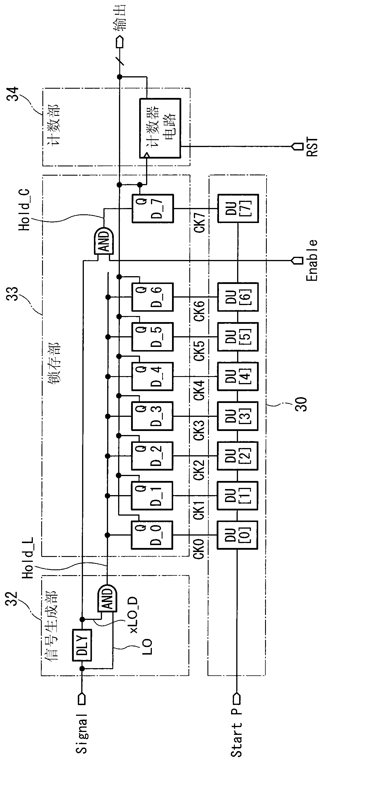
[0048] First, a first embodiment of the present invention will be described. figure 1 An example of the configuration of the time detection circuit of this embodiment is shown. Hereinafter, the configuration of this example will be described. figure 1 The shown time detection circuit is composed of a delay unit 30 , a signal generation unit 32 , a latch unit 33 , and a count unit 34 .

[0049] The delay unit 30 has a plurality of delay units DU[0] to DU[7] that delay an input signal and output it. Input the start pulse (=StartP) to the first delay unit DU[0].

[0050] The signal generation unit 32 generates control signals for controlling the operations of the latch unit 33 and the counter unit 34 . The signal generating section 32 has: an inversion delay circuit DLY that inverts and delays an analog signal Signal that is an object of time detection; and an AND circuit that outputs a signal that takes an input L0 (= Signal) and the logical product (AND) of the output xL0...

no. 2 approach )

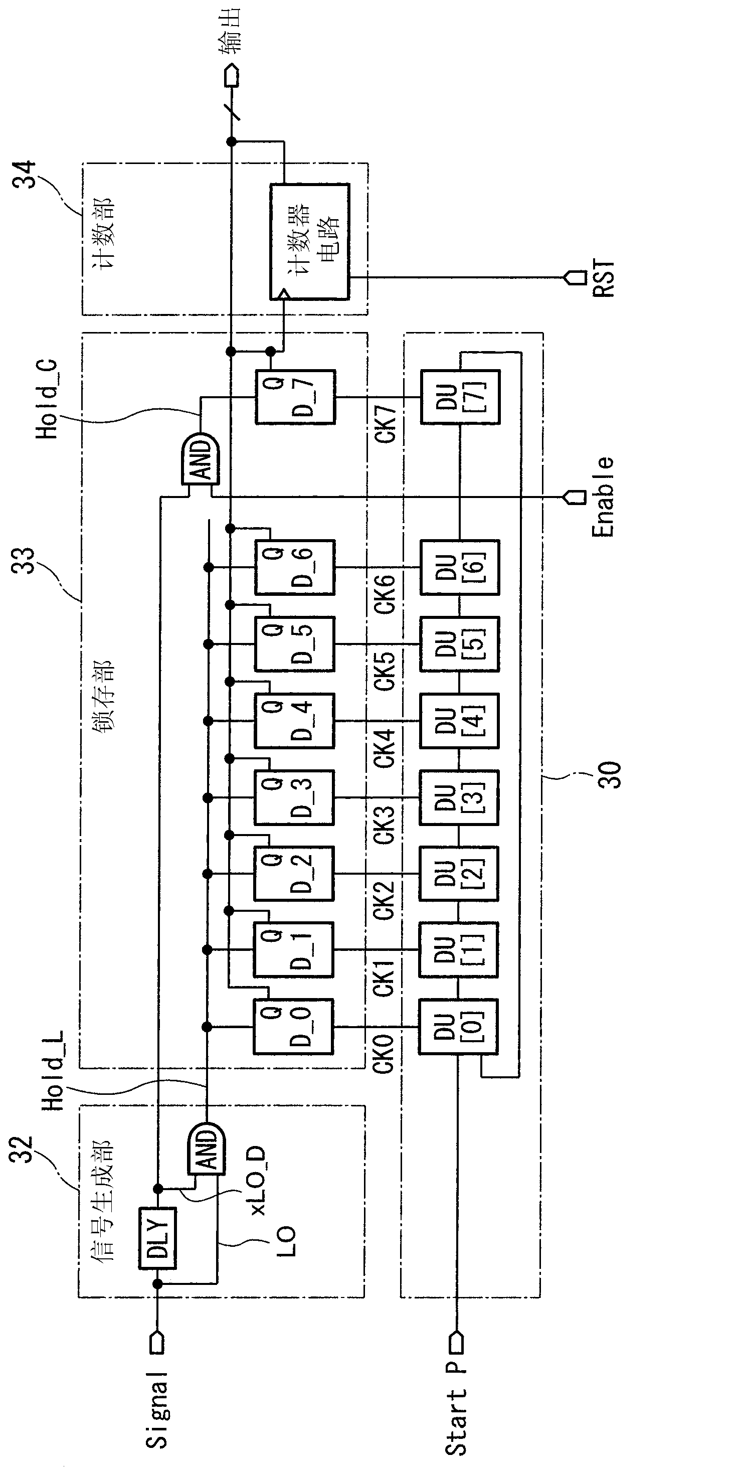
[0063] Next, a second embodiment of the present invention will be described. image 3 An example of the configuration of the time detection circuit of this embodiment is shown. The configuration diagram of this example will be described below. and figure 1 The structure shown in is different from the structure of the delay section 30 . In the present embodiment, a ring delay circuit is realized by connecting a plurality of delay units DU[*] (* is 0 to 7) constituting the delay unit 30 in a ring shape. In addition to figure 1 The same, so the description is omitted.

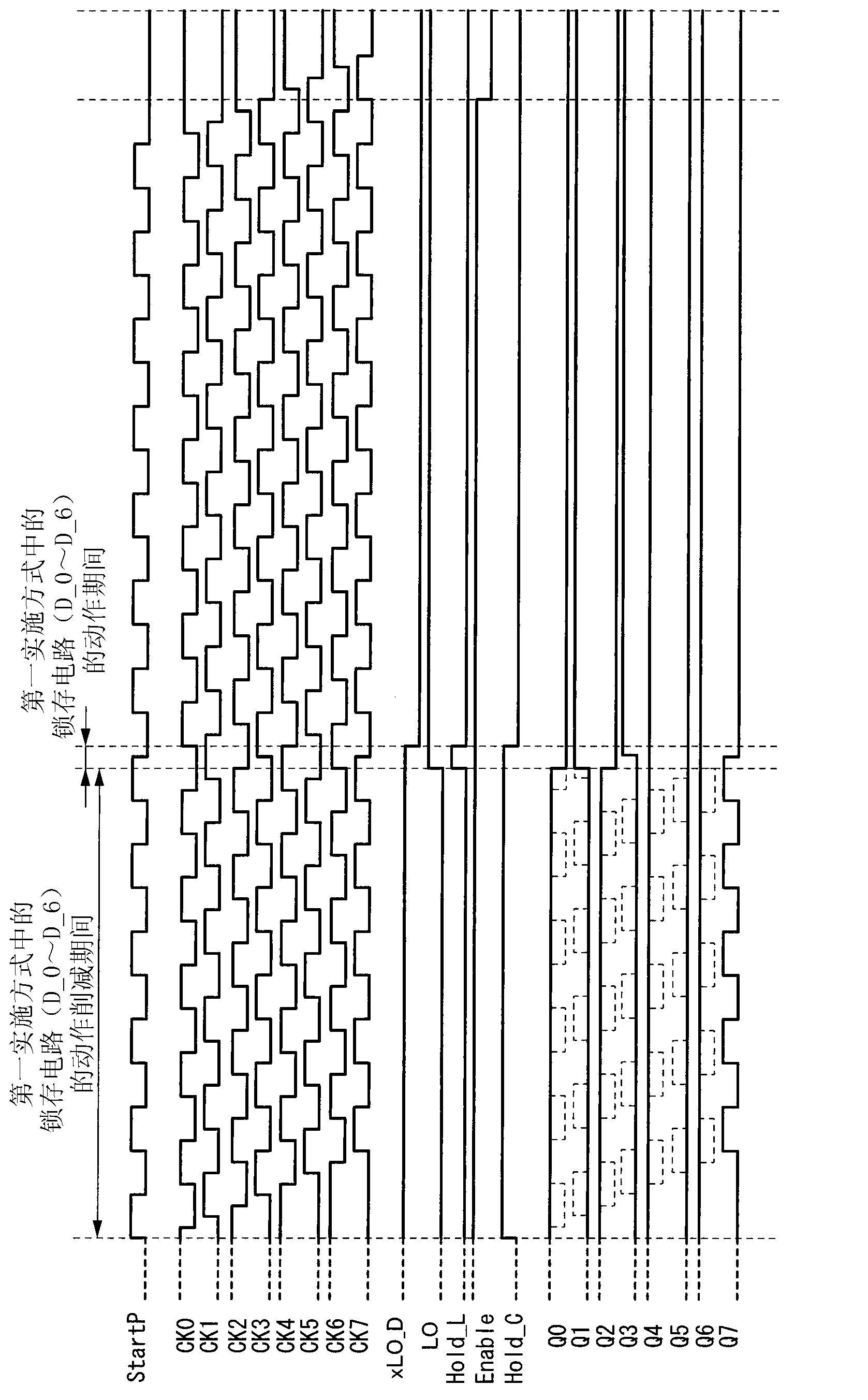
[0064] Next, the operation of this example will be described. Figure 4 The operation of the time detection circuit of this embodiment is shown. and figure 2 The difference is the start pulse (=StartP), the logic state of the start pulse (=StartP) changes from low level to high level, thus, the delay part 30 starts to operate, and according to the output CK7 from the delay part 30, The counting operatio...

no. 3 approach )

[0067] Next, a third embodiment of the present invention will be described. Figure 5 An example of the configuration of the time detection circuit of this embodiment is shown. Hereinafter, the configuration diagram of this example will be described. exist Figure 5 The illustration of the delay unit 30 is omitted. and image 3 The structure shown in is different in that a comparison unit 31 is added. The comparator 31 is composed of a voltage comparator which receives an analog signal Signal which is the object of time detection and a ramp wave Ramp which increases or decreases with the passage of time, and outputs a signal indicating a comparison between the analog signal Signal and the ramp wave Ramp. signal of the result. Thus, a time interval corresponding to the analog signal Signal (equivalent to figure 2 "Detected time" in the description of the ). In addition to image 3 The same, so the description is omitted.

[0068] Next, the operation of this example wi...


PUM


Abstract

The present invention is a time detection circuit having: a delay unit (30) that starts operation at a first timing relating to the input of a first pulse and that has a plurality of delay units (DU) that delay and output an input signal (Start P); a latch unit (33) that latches the logical state of the plurality of delay units (DU); a count unit (34) that counts on the basis of a clock (CK7) output from any one (DU[7]) of the plurality of delay units; and a latch control unit (32) that enables the latch unit (33) at a second timing relating to the input of a second pulse, and causes the latch unit to execute a latch at a third timing that lags from the second timing by a predetermined time. The latch circuits (D_0 to D_6) that configure the latch unit (33) maintain a disabled state (holding state) until the input of the second pulse (the interval of detected time), and so it is possible to reduce the electric current consumed by the latch unit (33).

Description

technical field [0001] The present invention relates to a time detection circuit, an AD converter and a solid-state imaging device using the time detection circuit. [0002] this application claims priority based on Japanese Patent Application No. 2010-177756 for which it applied to Japan on August 6, 2010, and uses the content here. Background technique [0003] As an example of a conventional time detection circuit, there is known Figure 8 The structure shown (for example, refer patent document 1, 2). first of all, yes Figure 8 The structure and operation of the time detection circuit will be described. [0004] Figure 8 The structure of the conventional time detection circuit is shown. Figure 8 The shown time detection circuit is composed of a delay unit 30 , a comparison unit 31 , a latch unit 33 , and a count unit 34 . The delay unit 30 has a plurality of delay units DU[0] to DU[7] that delay an input signal and output it. Input the start pulse (=StartP) to the f...

Claims


Application Information

Patent Timeline
Patent Type & Authority Applications(China)
IPC IPC(8): H03M1/12H04N5/374H04N5/378
CPCG04F10/005H03M1/56H04N25/767H04N25/75H01L27/14601H03K21/00H03M1/34
Inventor 萩原义雄
Owner OLYMPUS CORP
Why Eureka
Try Eureka