Method for reducing silicon etching loading effect

A technology of etching load and effect, applied in the direction of electrical components, semiconductor/solid-state device manufacturing, circuits, etc., to achieve the effect of improving silicon etching load effect and solving manufacturing process problems

Active Publication Date: 2013-04-24
SHANGHAI HUAHONG GRACE SEMICON MFG CORP
View PDF5 Cites 19 Cited by
  • Summary
  • Abstract
  • Description
  • Claims
  • Application Information

AI Technical Summary

Problems solved by technology

[0003] The technical problem to be solved by the present invention is to provide a method for reducing the load effect of silicon etching, to solve the manufacturing process problems of bipolar transistor buried layer connection and optical splitter, and realize its physical structure

Method used


Image

  • Method for reducing silicon etching loading effect
  • Method for reducing silicon etching loading effect
  • Method for reducing silicon etching loading effect

Examples


Embodiment 1

[0044] Embodiment 1 of the present invention mainly comprises following specific steps:

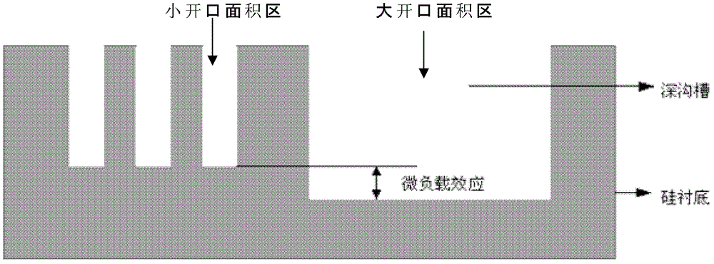
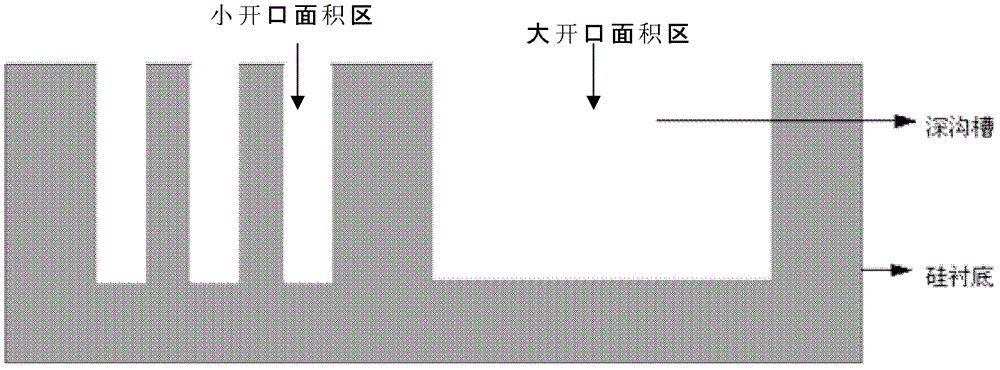
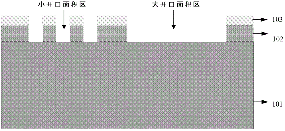
[0045] 1. If image 3 As shown, one or more dielectric films are deposited on the silicon substrate 101 as the hard mask layer 102, for example, a layer of dielectric film (such as an oxide film) can be deposited on the silicon substrate 101 as the hard mask layer 102, or An oxide film with a thickness of 125 angstroms and a SiN film with a thickness of 1500 angstroms are deposited on the silicon substrate 101 as the hard mask layer 102, because the oxide film acts as a buffer layer between the silicon substrate 101 and the SiN film, so image 3Only one film (ie, the hard mask layer 102, which includes an oxide film and a SiN film) is depicted in the figure. Then, the first photoresist 103 is coated, developed, and a pattern of the hard mask layer is formed, including a large opening area area and a small opening area area. The hard mask layer 102 is then etched, stopping on top of the ...

Embodiment 2

[0051] In order to achieve the purpose of removing the oxide film in the large opening area region and retaining the oxide film in the small opening area region, there is another alternative solution, that is, Example 2. Embodiment 2 mainly includes the following concrete steps:

[0052] 1. As Figure 5 As shown, one or more dielectric films are deposited on the silicon substrate 101 as the hard mask layer 102. For example, a dielectric film (such as an oxide film) may be deposited on the silicon substrate 101 as the hard mask layer 102, or A layer of oxide film with a thickness of 125 angstroms and a SiN film with a thickness of 1500 angstroms are deposited on the silicon substrate 101 as the hard mask layer 102, because the role of the oxide film is to serve as a buffer layer between the silicon substrate 101 and the SiN film, so image 3 Only one layer of film (ie hard mask layer 102, which includes oxide film and SiN film) is drawn in the middle; then the first photoresis...

Embodiment 3

[0057] Embodiment 3 of the present invention mainly includes the following specific steps:

[0058] 1. As image 3 As shown, one or more dielectric films are deposited on the silicon substrate 101 as the hard mask layer 102. For example, a dielectric film (such as an oxide film) may be deposited on the silicon substrate 101 as the hard mask layer 102, or A layer of oxide film with a thickness of 125 angstroms and a SiN film with a thickness of 1500 angstroms are deposited on the silicon substrate 101 as the hard mask layer 102, because the role of the oxide film is to serve as a buffer layer between the silicon substrate 101 and the SiN film, so image 3 Only one film (ie, the hard mask layer 102, which includes an oxide film and a SiN film) is depicted in the figure. Then, the first photoresist 103 is coated and developed to form a pattern of the hard mask layer, including a large opening area area and a small opening area area. The hard mask layer 102 is then etched, stopp...


PUM

PropertyMeasurementUnit
thicknessaaaaaaaaaa
thicknessaaaaaaaaaa
thicknessaaaaaaaaaa

Abstract

The invention discloses a method for reducing a silicone etching loading effect. The method comprises the following steps of (1) forming a groove hard mask layer image, (2) enabling a silicon substrate to espouse in a zone with large opening area and keeping part of dielectric films in a zone with small opening area, (3) growing silicone in the zone with the large opening area and growing no silicon in the zone with the small opening area, and (4) conducting groove etching to form a final groove image. The dielectric films like silicon oxide and silicon nitride are kept in the zone (the zone with the small opening area) where etching speed is low, mono-crystalline silicon is exposed in the zone (the zone with the large opening area) where the etching speed is fast, the silicone is grown in the zone with the large opening area by the utilization of a selective epitaxial method, the compensation dosage of the grown silicon is worked out according to etching load to enable the final depths, in zones with different opening area, of groove structures to be the same so as to improve the etching loading effect, and therefore the problems of buried layer connection of bipolar transistors and manufacturing technology of optical branching devices are solved, and physical structures of grooves are realized.

Description

technical field [0001] The invention belongs to the manufacturing process of semiconductor integrated circuits, in particular to a method for reducing the etching load effect. Background technique [0002] The size of the local opening area of ​​the photomask will have a great influence on the etching rate of silicon etching, so this loading effect is particularly obvious in silicon etching, especially in structures with a depth greater than 2um (micrometer), such as figure 1 As shown, in the silicon etching process, due to the difference in the local opening area, the etching depth in the area with a large opening area and the area with a small opening area are inconsistent, resulting in the micro-loading effect of etching. In some application fields such as bipolar transistor buried layer connection and optical splitter manufacturing process, the load effect of etching has become one of the main technical problems. Due to the existence of the basic physical principles of ...

Claims


Application Information

Patent Timeline
Patent Type & Authority Applications(China)
IPC IPC(8): H01L21/3065H01L21/205H01L21/311
Inventor 刘鹏吴智勇
Owner SHANGHAI HUAHONG GRACE SEMICON MFG CORP
Why Eureka
Try Eureka