Vertical parasitic type PNP triode and manufacture method

A PNP triode and vertical parasitic technology, which is applied in semiconductor/solid-state device manufacturing, transistors, electrical components, etc., can solve the problems of device size reduction, large collector connection resistance, and large device area, so as to reduce contact resistance and reduce collection The effect of electrode resistance and uniform diffusion distribution

Active Publication Date: 2015-04-08
SHANGHAI HUAHONG GRACE SEMICON MFG CORP
View PDF3 Cites 0 Cited by
  • Summary
  • Abstract
  • Description
  • Claims
  • Application Information

AI Technical Summary

Problems solved by technology

The disadvantage is that the device area is large and the connection resistance of the collector is large
Since the extraction of the collector electrode in the prior art is realized through another active region adjacent to the collector region, and the other active region and the collector region need to be isolated by STI or other field oxygen, such This greatly limits the further reduction of the device size

Method used


Image

  • Vertical parasitic type PNP triode and manufacture method
  • Vertical parasitic type PNP triode and manufacture method
  • Vertical parasitic type PNP triode and manufacture method

Examples


Embodiment Construction

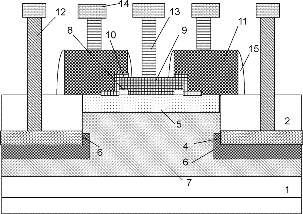
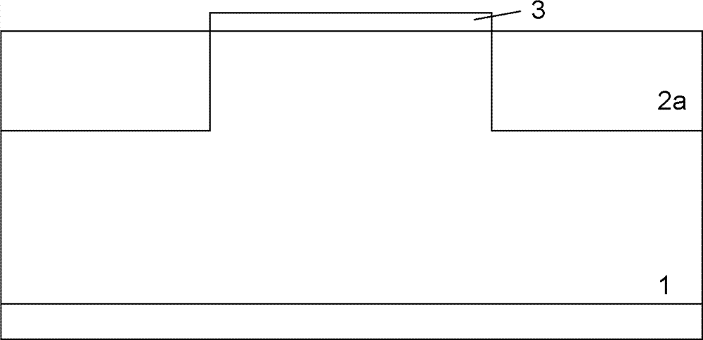
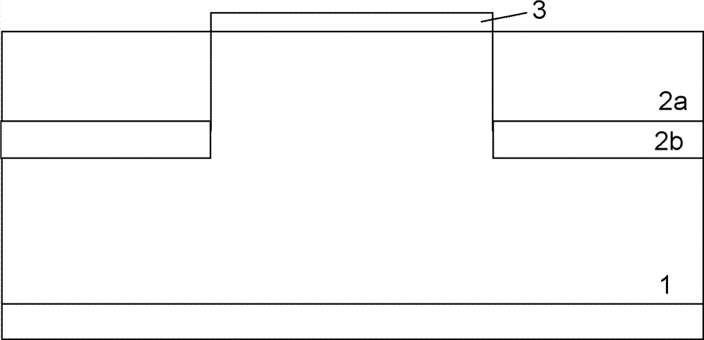
[0029] Such as figure 1 As shown, it is a schematic structural diagram of a vertical parasitic PNP transistor device according to an embodiment of the present invention. An N-type deep well 1 is formed on a P-type silicon substrate. In the N-type deep well 1, the isolation structure on the silicon substrate is shallow trench isolation, that is, the active region is isolated by shallow trench field oxygen 2 .

[0030] The collector region 7 of the vertical parasitic PNP transistor is composed of a P-type ion implantation region formed in the active region, the depth of the collector region 7 is greater than the depth of the bottom of the shallow trench field oxygen 2, and The collector region 7 extends laterally into the bottom of the shallow trench field oxygen 2 on both sides of the active region. A groove is formed at the bottom of the shallow groove field oxygen 2 on the peripheral side of the active region, the width of the groove is less than or equal to the width of the...


PUM

PropertyMeasurementUnit
thicknessaaaaaaaaaa

Abstract

The invention discloses a vertical parasitic type PNP triode. A groove is formed in the bottom portion of shallow shot field oxygen on the circumferential side of an active region, and is filled with polycrystalline silicon, the polycrystalline silicon filling in the groove forms a polycrystalline silicon buried layer, P-type impurities are mixed in the polycrystalline silicon buried layer, and the P-type impurities further spread to silicon substrate on the circumferential side of the polycrystalline silicon buried layer to form a first P-type doped region. The polycrystalline silicon buried layer and the doped region form a collector connecting layer, and the collector connecting layer contacts with a collecting region on the bottom portion of the shallow slot field oxygen. Deep holes are formed in the shallow slot field oxygen on the upper portion of the polycrystalline silicon buried layer and contact with and lead out collectors. The invention further discloses a manufacture method of the vertical parasitic type PNP triode. The vertical parasitic type PNP triode and the manufacture method of the vertical parasitic type PNP triode can improve the thickness of the collector connecting layer, and enable the impurities to be distributed evenly, can reduce the resistance and the contact resistance of the collector collecting layer and enable resistance values to be even, and therefore can improve the cut-of frequency of a device.

Description

technical field [0001] The invention relates to the field of semiconductor integrated circuit manufacturing, in particular to a vertical parasitic PNP transistor; the invention also relates to a method for manufacturing the vertical parasitic PNP transistor. Background technique [0002] In RF applications, higher and higher device characteristic frequencies are required. In BiCMOS process technology, NPN transistors, especially silicon germanium (SiGe) heterojunction transistors (HBT) or germanium silicon carbon heterojunction transistors (SiGeC HBT) are good choices for UHF devices. And the SiGe process is basically compatible with the silicon process, so SiGe HBT has become one of the mainstreams of UHF devices. In this context, the requirements for the output device are correspondingly increased, such as having a certain current gain coefficient and cut-off frequency. [0003] In the prior art, the output device can adopt a vertical parasitic PNP transistor. In the exi...

Claims


Application Information

Patent Timeline
Patent Type & Authority Patents(China)
IPC IPC(8): H01L29/73H01L29/737H01L29/06H01L29/08H01L21/331
Inventor 陈帆陈雄斌薛凯周克然潘嘉李昊蔡莹陈曦
Owner SHANGHAI HUAHONG GRACE SEMICON MFG CORP
Why Eureka
Try Eureka