Edge protection method for achieving growth of semiconductor material having self-peeling function

An edge protection and self-stripping technology, applied in crystal growth, semiconductor/solid-state device manufacturing, single crystal growth, etc. Commercial promotion, practical effect

Inactive Publication Date: 2013-05-01
CHINA ELECTRONICS TECH GRP NO 46 RES INST
View PDF9 Cites 5 Cited by
  • Summary
  • Abstract
  • Description
  • Claims
  • Application Information

AI Technical Summary

Problems solved by technology

[0003] The invention provides an edge protection method for realizing the growth of a semiconductor material with a self-stripping function, which is used to solve the problems in the prior art that the growing polycrystalline crystals on the edge of the wafer are not easy to separate, and cracks are easily generated under the influence of stress, thereby affecting the integrity of the wafer.

Method used


Image

  • Edge protection method for achieving growth of semiconductor material having self-peeling function
  • Edge protection method for achieving growth of semiconductor material having self-peeling function
  • Edge protection method for achieving growth of semiconductor material having self-peeling function

Examples


Embodiment Construction

[0031] The following will clearly and completely describe the technical solutions in the embodiments of the present invention with reference to the accompanying drawings in the embodiments of the present invention. Obviously, the described embodiments are only some, not all, embodiments of the present invention. Based on the embodiments of the present invention, all other embodiments obtained by persons of ordinary skill in the art without making creative efforts belong to the protection scope of the present invention.

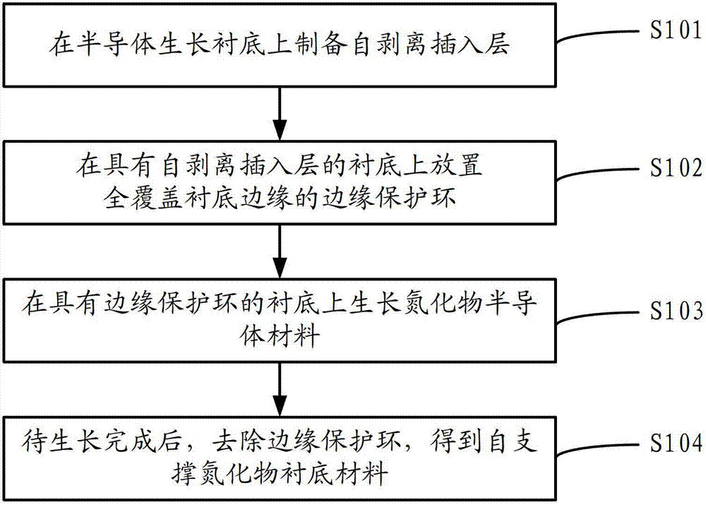
[0032] In order to solve the problems existing in the prior art, an embodiment of the present invention provides an edge protection method for realizing the growth of a semiconductor material with a self-stripping function, such as figure 1 As shown, the method includes:

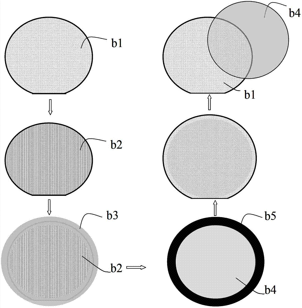
[0033] Step S101, preparing a self-stripping insertion layer on a semiconductor growth substrate;

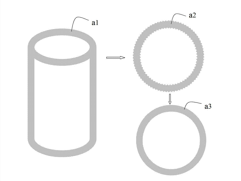
[0034] Step S102, placing an edge protection ring fully covering the edge of the substrat...


PUM

PropertyMeasurementUnit
thicknessaaaaaaaaaa

Abstract

The present invention discloses an edge protection method for achieving growth of a semiconductor material having a self-peeling function. The method comprises: preparing a self-peeling inserting layer on a semiconductor growth substrate; placing an edge protection ring completely covering the substrate edge on the substrate having the self-peeling inserting layer; growing a nitride semiconductor material on the substrate having the edge protection ring; and removing the edge protection ring after completing the growth to obtain the self-supporting nitride substrate material. With the edge protection method, the problem of poor self-supporting nitride substrate integrity affected by edge effect, polycrystalline deposition and the like during self-peeling nitride substrate preparation in the prior art is solved.

Description

technical field [0001] The invention relates to the field of semiconductor material growth, in particular to an edge protection method for realizing the growth of semiconductor materials with self-stripping function. Background technique [0002] The third-generation semiconductor materials represented by nitrides are direct band gap semiconductors, which have the advantages of large band gap, high electron saturation velocity, and small dielectric constant. Excellent properties such as high electron mobility, high breakdown electric field, and chemical stability allow it to work under harsh conditions and are suitable for the preparation of various devices. They are widely used in optoelectronic devices such as laser diodes, ultraviolet detectors, and light-emitting diodes. GaN materials are representative examples. In terms of optoelectronic devices, blue light sources can be used for deep-sea communication, and blue light lasers can be used for detection and identificati...

Claims


Application Information

Patent Timeline
Patent Type & Authority Applications(China)
IPC IPC(8): C30B25/16C30B25/18H01L21/02
Inventor 徐永宽杨丹丹张嵩程红娟李晖徐所成张丽王迪兰飞飞张政史月增
Owner CHINA ELECTRONICS TECH GRP NO 46 RES INST
Why Eureka
Try Eureka