
Manufacturing method of nanoscale super resolution optical focusing device

An optical focusing and nanoscale technology, applied in the direction of nanotechnology, diffraction grating, etc., can solve the problems of low transmission efficiency and weak focal spot intensity, and achieve the effects of improved integration, simple structure and broad application prospects

Inactive Publication Date: 2013-05-01
INST OF OPTICS & ELECTRONICS - CHINESE ACAD OF SCI
View PDF2 Cites 17 Cited by
  • Summary
  • Abstract
  • Description
  • Claims
  • Application Information

AI Technical Summary

Problems solved by technology

In a series of new focusing devices, such as hypergratings, the focusing effect of the Fresnel zone plate and the super-resolution characteristics of the multilayer nanofilm are used to obtain a small focal spot, but its transmission efficiency is very low. The intensity of the focal spot is very weak, and the focal spot is focused inside the multilayer film

Method used


Image

  • Manufacturing method of nanoscale super resolution optical focusing device
  • Manufacturing method of nanoscale super resolution optical focusing device
  • Manufacturing method of nanoscale super resolution optical focusing device

Examples


Embodiment Construction

[0022] The present invention will be described in detail below in conjunction with the accompanying drawings and specific embodiments, but the scope of protection of the present invention is not limited to the following examples, but should include all content in the claims.

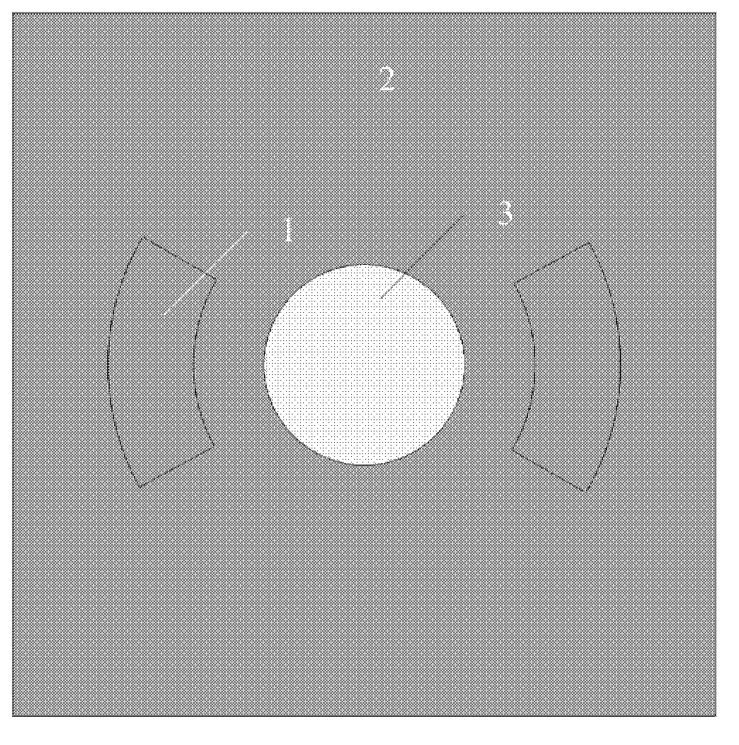
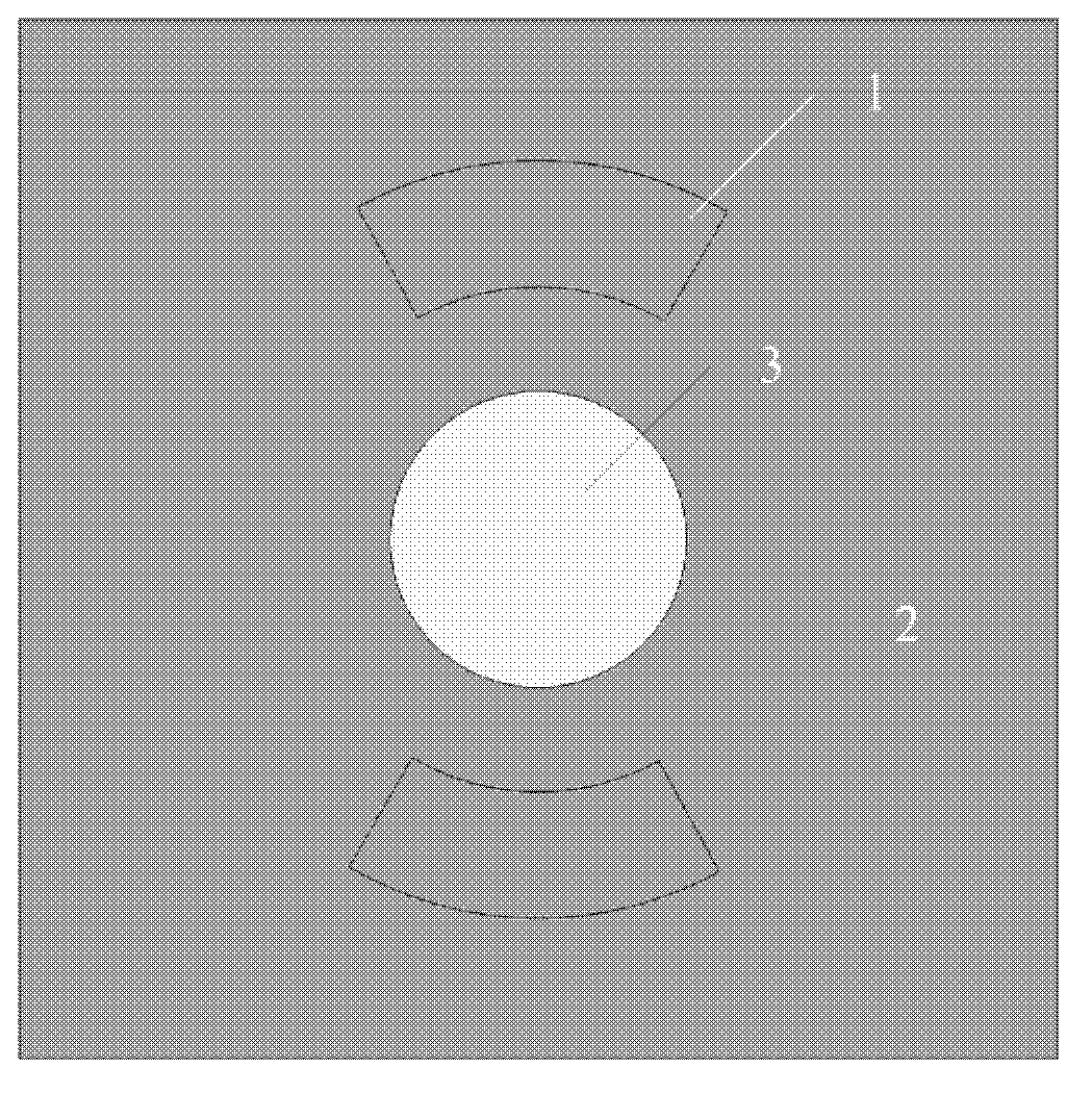
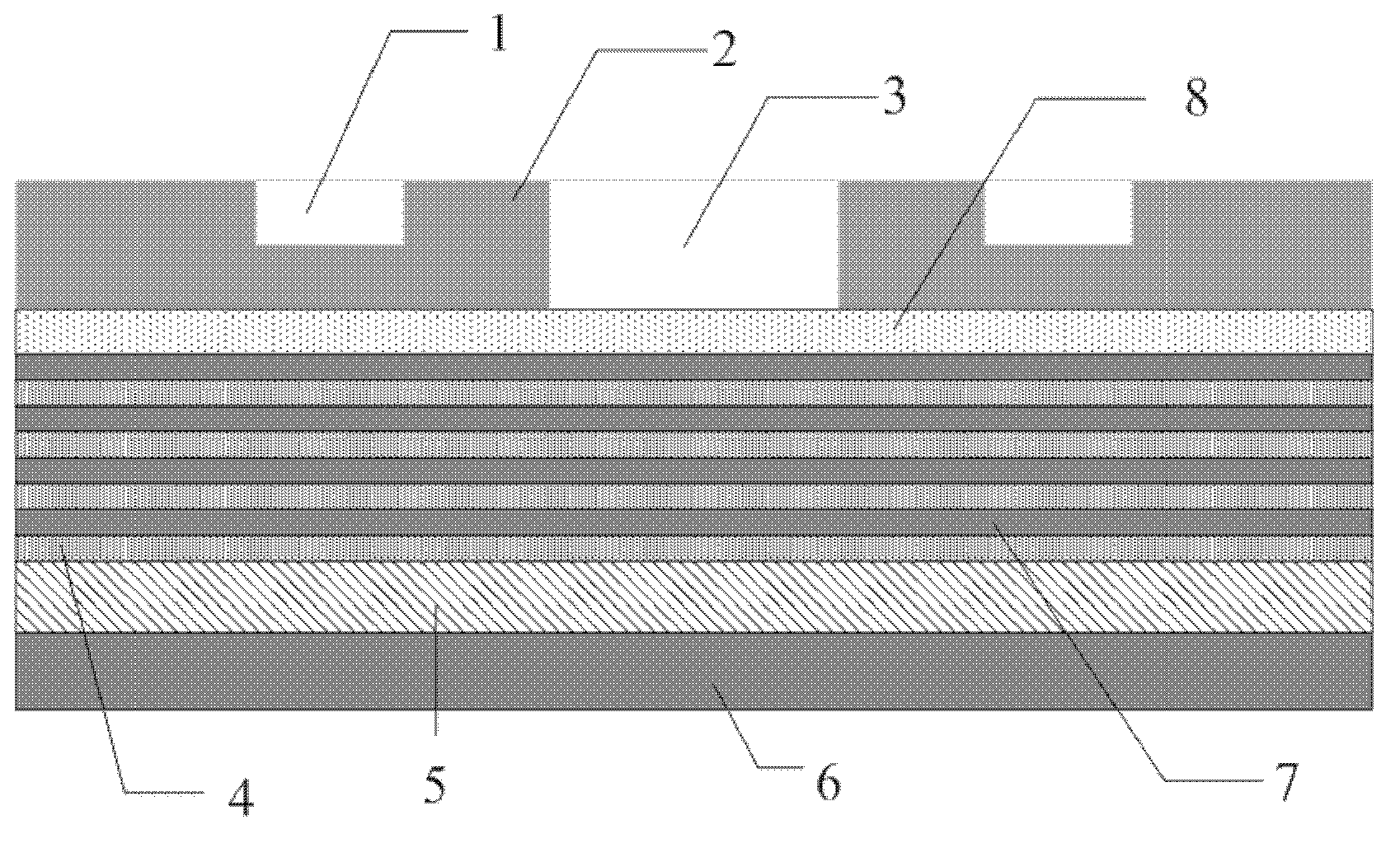
[0023] figure 2 shows the fabrication of nanoscale super-resolution optical focusing devices, figure 2 Among them, 1 is the groove annular zone, 2 is the metal film, 3 is the Fresnel first-order wave zone circular hole, 4 is the dielectric film, 5 is the photoresist, 6 and 7 are the metal film, and 8 is the substrate. The metal film 2, the dielectric film 4, the photoresist 5, the metal films 6 and 7, and the substrate 8 are all closely arranged up and down.

[0024] The present invention implements the fabrication method of the nanoscale super-resolution optical focusing device, comprising the following steps:

[0025] Step S1: select the working wavelength λ of the incident light, and select the ma...


PUM


Abstract

The invention relates to a manufacturing method of a nanoscale super resolution optical focusing device, which comprises the following steps that S1 an operating wavelength of incident light is selected, a euphotic substrate is selected, a metal film is evaporated and coated on a surface, and the incident light is perpendicular to the upper surface of the metal film; S2 materials of the metal film and a dielectric film are selected in accordance with the operating wavelength, and fresnel wavezone radii at all levels are designed; S3 the position of a groove band, i.e. the radius of an inner ring, is selected; S4 the width and the depth of the groove band are modulated in accordance with the requirement of the intensity of focal spots; S5 the orientation of the groove band is selected in accordance with a polarization state of the incident light; S6 a processing technique is utilized to obtain metal masks of fresnel wavezone annular gaps and grooves; S7 nanometer-thick metal and dielectric multilayer film structures are alternately evaporated and coated on back surfaces of the metal masks, and the total thickness of a multilayer film is deposited as a focal length of a lens; and S8 a layer of nanometer-thick photoresist and a layer of reflecting metal layer are evaporated and coated on the multilayer film structures, and then the nanoscale super resolution optical focusing device is obtained.

Description

technical field [0001] The invention relates to a focusing element including a metal nano-round hole or an annulus, in particular to a nanoscale super-resolution optical focusing device. Background technique [0002] In recent years, nanotechnology has developed by leaps and bounds, and its application in lithography and other aspects also puts forward new requirements for corresponding resolution. Various focusing devices are gradually developing towards miniaturization and integration. In a series of new focusing devices, such as hypergratings, the focusing effect of the Fresnel zone plate and the super-resolution characteristics of the multilayer nanofilm are used to obtain a small focal spot, but its transmission efficiency is very low. The intensity of the focal spot is very weak, and the focal spot is focused inside the multilayer film. Contents of the invention [0003] The technical problem to be solved by the present invention is to enhance the transmission effic...

Claims


Application Information

Patent Timeline
Patent Type & Authority Applications(China)
IPC IPC(8): G02B5/18B82Y40/00
Inventor 罗先刚赵泽宇王长涛陶兴王彦钦高平胡承刚黄成杨欢姚纳
Owner INST OF OPTICS & ELECTRONICS - CHINESE ACAD OF SCI
Learn More