Device structure of power diode

A technology of power diode and device structure, applied in the direction of semiconductor devices, electrical components, circuits, etc., can solve the problems of increasing manufacturing cost, affecting the conduction ability of devices, and easily polluting equipment, etc., to reduce losses, high withstand voltage, and improve Turn on the effect of speed

Active Publication Date: 2013-05-08
SHANGHAI HUAHONG GRACE SEMICON MFG CORP
View PDF3 Cites 0 Cited by
  • Summary
  • Abstract
  • Description
  • Claims
  • Application Information

AI Technical Summary

Problems solved by technology

However, due to the existence of defects, it will affect the conduction ability of the device when it is turned on; and the use of gold or platinum heavy metals will not only easily pollute the equipment, but also increase the manufacturing cost

Method used


Image

  • Device structure of power diode
  • Device structure of power diode
  • Device structure of power diode

Examples


Embodiment Construction

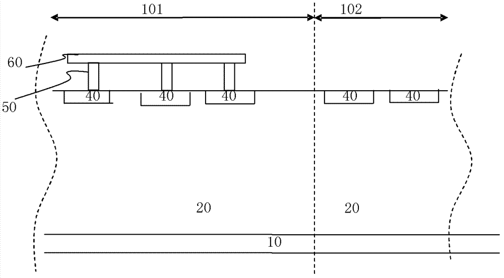
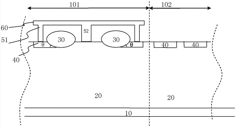
[0031] Such as figure 2 As shown, the device structure of the power diode of the present invention includes a cell 101 and a terminal area 102, and the terminal area 102 is arranged on the periphery of the cell 101;

[0032] The cathode of the device is drawn from the back of the device, and above the cathode of the device is the N-type substrate 10 of the terminal region 102 and the cell 101, and above the N-type substrate 10 is the N-type epitaxial region 20;

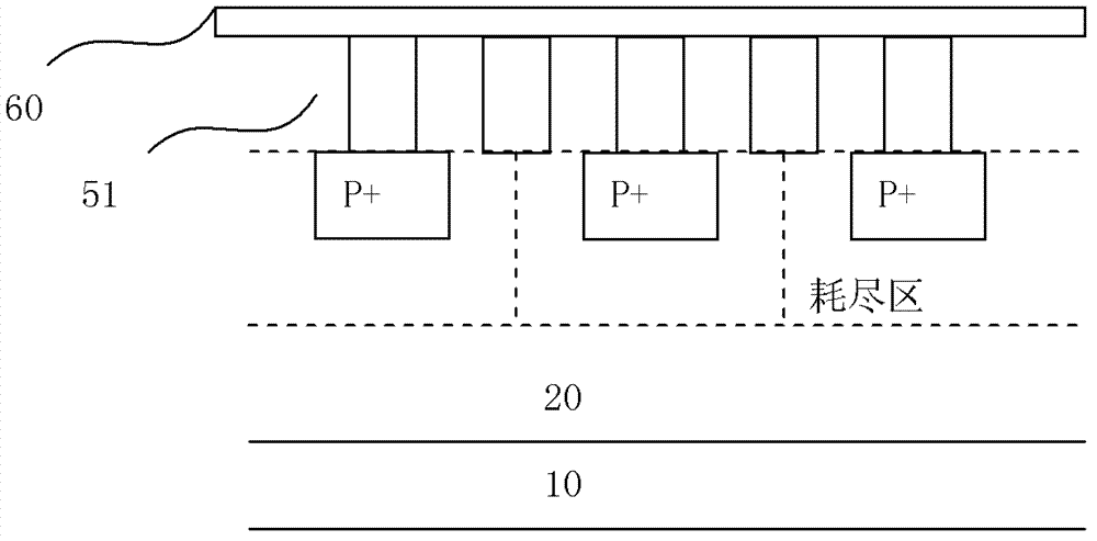
[0033] The anode of the device is located on the surface of the N-type epitaxial region 20, and a plurality of P-type heavily doped regions 40 are distributed in the N-type epitaxial region 20, and the P-type heavily doped regions 40 and the N-type epitaxial regions 20 are alternately arranged at intervals;

[0034] The shape of the P-type heavily doped region 40 may be one or more of square, circular, rectangular, and hexagonal.

[0035] There are metal leads 60 above the anode of the device, and the metal leads 60...


PUM


Abstract

The invention discloses a device structure of a power diode. A metal lead is located above the power diode of the device, and the metal lead is respectively alternated and contacted with a P type heavily doped region and a N type epitaxial region inside a cellular area through a doped region contacting hole and an epitaxial region contacting hole; the metal lead, the doped region contacting hole, the P type doped region, the N type epitaxial region and a N type substrate form a positive-intrinsicnegative (PIN) power diode; and the metal lead, the epitaxial region contacting hole, the N type extaxial region and the N type substrate form a schottky diode. A field oxide film is located between the P type heavily doped region and the N type epitaxial region, and an inclined angle which is not larger than 30 degrees is formed between the surface of the field oxide film and the horizontal direction of the P type heavily doped region. According of the device structure, high voltage-resistance capability of the power diode device can be achieved, rapid opening can be achieved, rapid recovery can be achieved when the power diode device is switched off reversely, and switching loss is reduced.

Description

technical field [0001] The invention relates to a semiconductor device structure, in particular to a device structure of a power diode. Background technique [0002] Power diode devices are the intrinsic driving force of the ever-evolving power-electronic systems, which have the advantages of energy saving, dynamic control, and noise reduction. Power semiconductors are mainly used to control the energy between the energy source and the load, and should have the characteristics of high precision, fast speed and low power consumption. [0003] Existing PIN(P + -N - -N + ) Diodes such as figure 1 As shown, it includes a cell 101 and a terminal area 102, and the terminal area 102 is arranged on the periphery of the cell 101; the cathode of the device is drawn from the back of the device, and above the cathode of the device is the N-type substrate 10 of the terminal area 102 and the cell 101, Above the N-type substrate 10 is an N-type epitaxial region 20; the anode of the de...

Claims


Application Information

Patent Timeline
Patent Type & Authority Applications(China)
IPC IPC(8): H01L29/861H01L29/872H01L29/868H01L29/06
Inventor 胡晓明
Owner SHANGHAI HUAHONG GRACE SEMICON MFG CORP
Why Eureka
Try Eureka