Method for decreasing series resistors of P type substrate hetero junction with intrinsic thin layer (HIT) solar cell

A technology for solar cells and substrates, applied in circuits, photovoltaic power generation, electrical components, etc., can solve problems such as reducing battery open circuit voltage and increasing series resistance

Inactive Publication Date: 2013-05-08
TRINASOLAR CO LTD
View PDF3 Cites 7 Cited by
  • Summary
  • Abstract
  • Description
  • Claims
  • Application Information

AI Technical Summary

Problems solved by technology

A higher barrier height reduces the open circuit voltage of the cell and also increases the series resistance

Method used


Image

  • Method for decreasing series resistors of P type substrate hetero junction with intrinsic thin layer (HIT) solar cell
  • Method for decreasing series resistors of P type substrate hetero junction with intrinsic thin layer (HIT) solar cell

Examples


Embodiment Construction

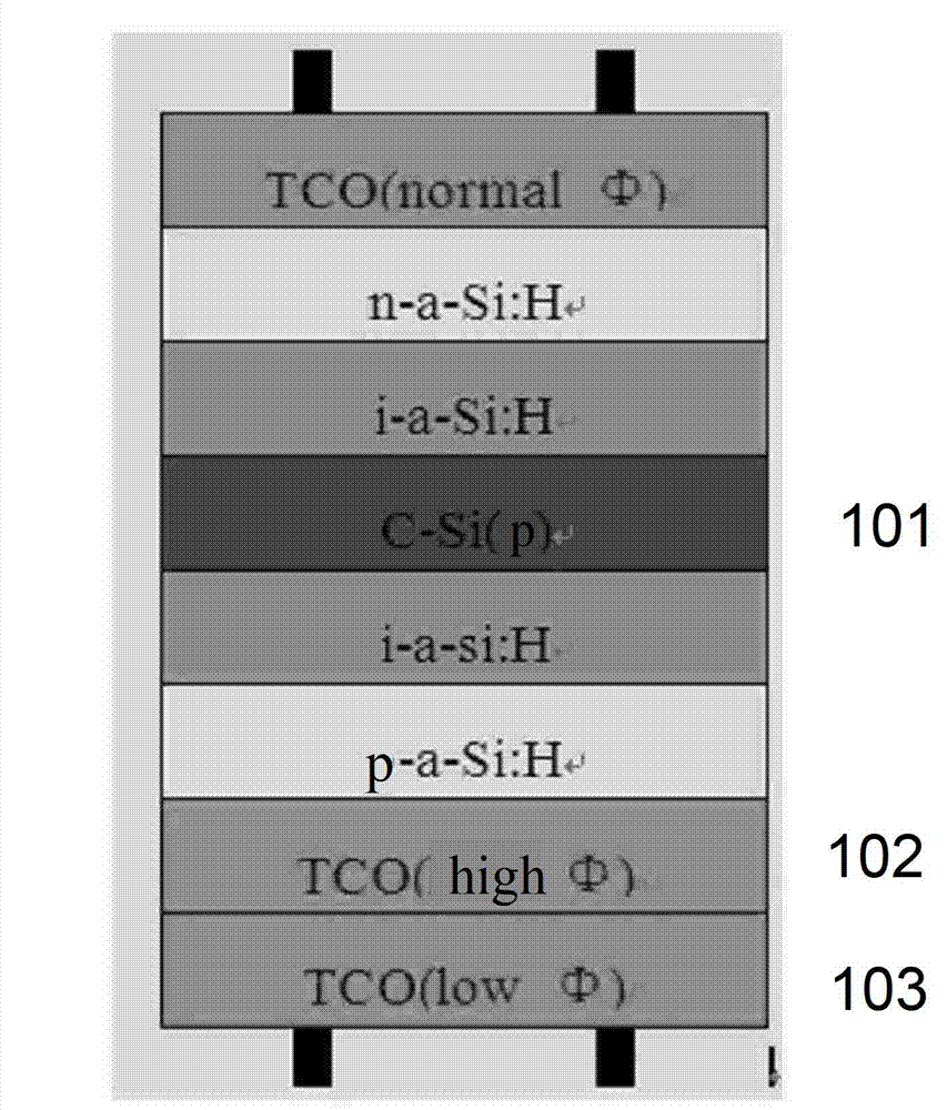
[0019] P-type substrate HIT battery:

[0020] Such as figure 1 As shown, an embodiment of the present invention uses a P-type silicon wafer to make a P-type substrate HIT cell. Compared with the existing P-type substrate HIT battery, the main difference is that the outside of the p-a-si:H layer (the side opposite to the middle P-type substrate 101) is sequentially covered with a high work function TCO layer 102 and a low work function TCO layer 103 .

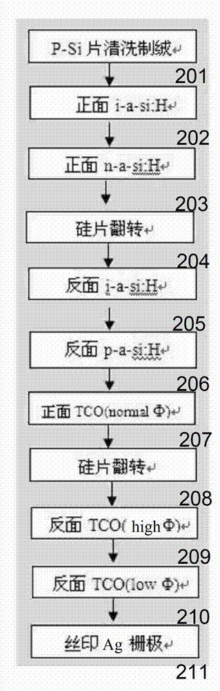
[0021] figure 1 An exemplary fabrication method for the shown P-type substrate HIT cell is described in figure 2 middle. Firstly, the p-type silicon wafer is strictly cleaned and textured (201), and then the PECVD method is used to deposit and grow i-a-si:H of about 1-10nm and n-a-si:H of about 1-10nm (202 and 203 ); then turn over the silicon wafer ( 204 ), on the other side of the silicon wafer, still use PECVD method to deposit and grow 1-10nm i-a-si:H and 10-20nm p-a-si:H ( 205 and 206 ). Then use the reactive plasma ...


PUM

PropertyMeasurementUnit
Work functionaaaaaaaaaa

Abstract

The invention discloses a method for decreasing series resistors of a P type substrate hetero junction with intrinsic thin layer (HIT) solar cell. The P type HIT solar cell comprises a P type crystalline silicon substrate layer, a first intrinsic non-crystalline silicon layer, a second intrinsic non-crystalline silicon layer, a N type non-crystalline silicon layer, a P type non-crystalline silicon layer, a first transparent conductive oxide (TCO ) layer and an electrode, a second TCO layer and an electrode. The first intrinsic non-crystalline layer and the second intrinsic non-crystalline layer are arranged on two sides of the P type crystalline silicon substrate layer, the N type non-crystalline layer is arranged on the outer side of the first intrinsic non-crystalline silicon layer, the P type non-crystalline silicon layer is arranged on the outer side of the second intrinsic non-crystalline silicon layer, the first TCO layer and the electrode are arranged on the outer side of the N type non-crystalline silicon layer, and the second TCO layer and the electrode are arranged on the outer side of the P type non-crystalline silicon layer, wherein the second TCO layer is a lamination layer composed of a high work function TCO layer and a low work function TCO layer, and the high work function TCO layer contacts with the P type non-crystalline silicon layer. At the same time, the invention discloses a corresponding method for formation of the solar cell.

Description

technical field [0001] The invention relates to the technical field of thin film solar cells. In particular, the present invention discloses a technique for reducing the series resistance of a P-type substrate HIT solar cell. Background technique [0002] HIT (Heterojunction with intrinsic Thinlayer) solar cells have attracted more and more attention due to their high efficiency, no need for complicated preparation processes, and small temperature coefficient. Usually the structure of the HIT battery is Ag / TCO / p-a-si:H / i-a-si:H / c-Si(n) / i-a-si:H / n-a-si:H / TCO / Ag (according to the customary expression in the art Method: a-si means amorphous silicon film, which means amorphous silicon film, c-si means crystal silicon means crystalline silicon, i means intrinsic type, p means P type, n means N type, H means hydrogenation; further, the above In the HIT battery structure, p-a-si:H means P-type hydrogenated amorphous silicon film, i-a-si:H means intrinsic hydrogenated amorphous si...

Claims


Application Information

Patent Timeline
IPC IPC(8): H01L31/0747H01L31/0224H01L31/20
CPCY02E10/50Y02P70/50
Inventor 崔艳峰袁声召石建华陆中丹孟凡英刘正新
Owner TRINASOLAR CO LTD
Why Eureka
Try Eureka