
Micro capacitance-type wall shear stress sensor and manufacturing method thereof based on through silicon via (TSV) technology

A micro-capacitor and through-silicon via technology, applied in the field of sensors, can solve the problems of unfavorable sensor integration with IC process 3D packaging, easy introduction of interference in packaging methods, insufficient bonding strength, etc. The effect of reducing package size

Inactive Publication Date: 2013-05-22
NORTHWESTERN POLYTECHNICAL UNIV
View PDF5 Cites 19 Cited by
  • Summary
  • Abstract
  • Description
  • Claims
  • Application Information

AI Technical Summary

Problems solved by technology

[0008] The purpose of the present invention is to provide a method based on the insufficient bonding strength of the MEMS capacitive shear stress sensor packaged by the traditional planar packaging process, the packaging method is easy to introduce interference, and it is not conducive to the 3D packaging integration of the sensor and the IC process. Miniature capacitive wall shear stress sensor with back hole connection of through-silicon via technology and manufacturing method thereof

Method used


Image

  • Micro capacitance-type wall shear stress sensor and manufacturing method thereof based on through silicon via (TSV) technology
  • Micro capacitance-type wall shear stress sensor and manufacturing method thereof based on through silicon via (TSV) technology
  • Micro capacitance-type wall shear stress sensor and manufacturing method thereof based on through silicon via (TSV) technology

Examples


Embodiment Construction

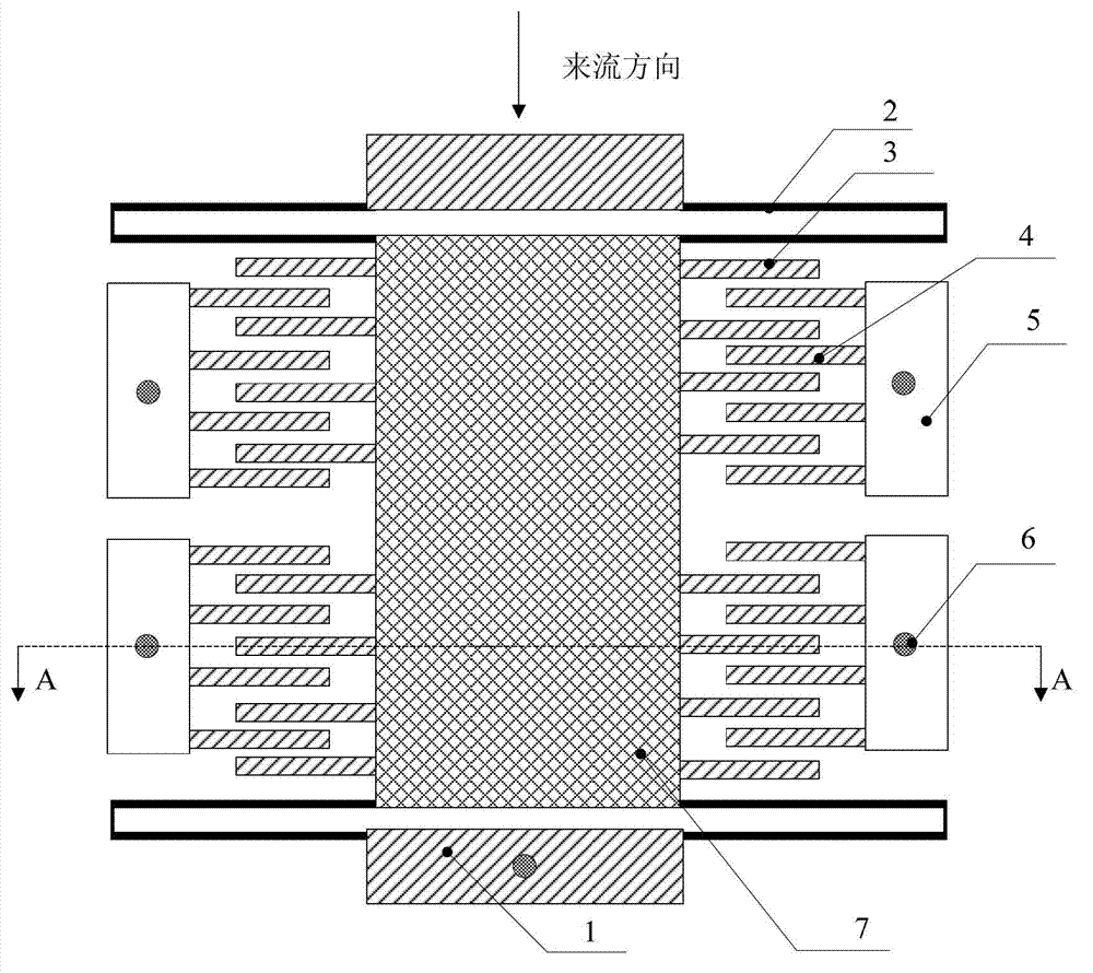
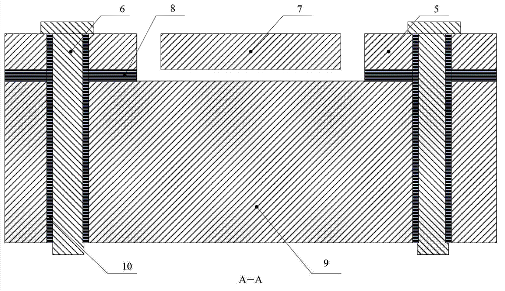
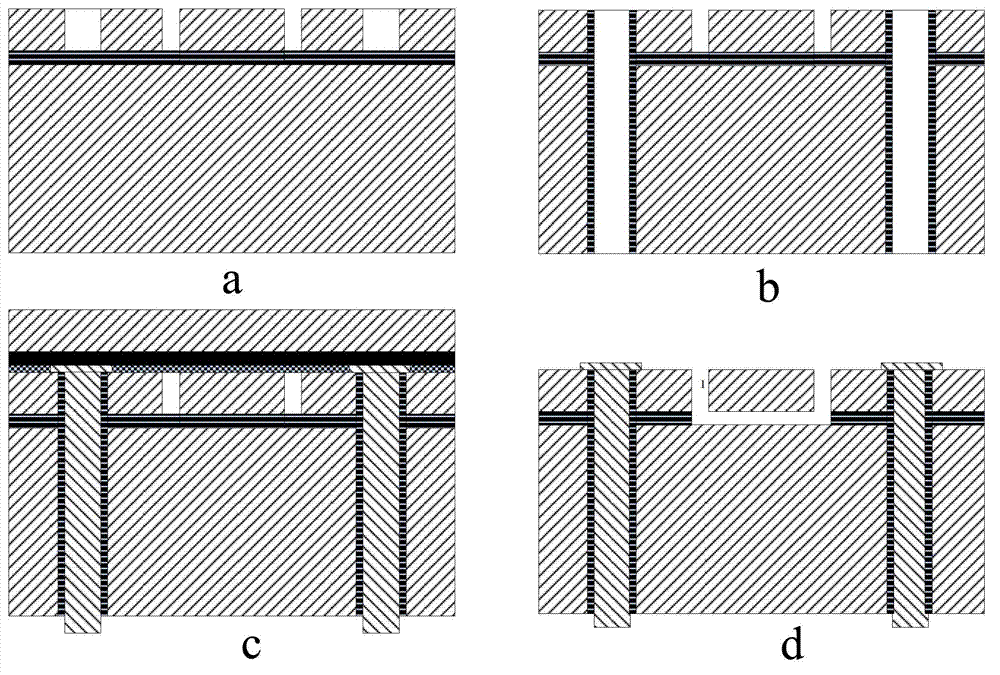
[0028] The miniature capacitive wall shear stress sensor based on the back hole connection of the through-silicon via technology in this embodiment mainly includes a floating unit anchor point 1, an elastic beam 2, a movable comb tooth 3, a fixed comb tooth 4, and a fixed comb tooth anchor point 5, TSV lead wire 6, floating unit 7, sacrificial layer 8, base layer 9 and TSV electrical insulation layer 10; the floating unit 7, elastic beam 2, movable comb 3, fixed comb 4 and anchor point are made The overall processing process is obtained, the electrical connection TSV is completed by electroplating, and the entire sensor is left-right symmetrical; the floating unit 7 and the movable comb 3 are connected to the anchor point 1 of the floating unit through the elastic beam 2, and are suspended on the base layer 9; the fixed comb 4 Connected to the fixed comb anchor point 5, the movable comb tooth 3 and the fixed comb tooth 4 form a capacitor, the TSV lead 6 forms electrical contact...


PUM


Abstract

The invention discloses a micro capacitance-type wall shear stress sensor and a manufacturing method of the micro capacitance-type wall shear stress sensor based on through silicon via (TSV) technology, and belongs to the technical field of sensors. The micro capacitance-type wall shear stress sensor comprises a floating unit anchor point 1, an elastic beam 2, a movable broach 3, a fixed broach 4, a fixed broach anchor point 5, a TSV lead 6, a floating unit 7, a sacrificial layer 8, a substrate layer 9 and a TSV electric insulation layer 10, and is manufactured through a micro machining process and a metal plating process. According to the micro capacitance-type wall shear stress sensor based on the TSV technology, the original lead bonding process is replaced by a back-surface lead process, so that the metal leas is prevented from being exposed in a flow filed to generate interference. The packaging size of the sensor is reduced, arraying of the sensor is benefited, and three-dimensional (3D) packaging of the sensor and an integrated circuit is benefited. A measurement device does not invade in the flow field, so that no-invasion-type wall shear stress measurement can be carried out on the flow field.

Description

[0001] Field: [0002] The invention relates to a miniature capacitive wall shear stress sensor and a manufacturing method thereof, in particular to a miniature capacitive wall shear stress sensor connected by a back hole based on through-silicon via technology, which belongs to the technical field of sensors. Background technique: [0003] The flow parameters near the wall, especially the wall shear stress, are important parameters for studying and judging the shape of the flow field and the state of the boundary layer. Conventional sensors for measuring shear stress mainly include friction balances, Preston tubes, Stanton tubes, and the like. Restricted by processing methods, its size is large, its dynamic range is narrow, and there are disadvantages such as signal lag to varying degrees. In addition, the shear stress sensors made by the traditional process are not easy to form an array, and it is impossible to realize the distributed measurement of the wall shear stress. ...

Claims


Application Information

Patent Timeline
IPC IPC(8): G01L1/14B81C1/00
Inventor 马炳和项志杰邓进军
Owner NORTHWESTERN POLYTECHNICAL UNIV
Learn More