Device and method for compensating dark current of image sensor
An image sensor and compensation device technology, applied in image communication, television, electrical components, etc., can solve the problem of reducing the frame rate of the sensor, save chip area and power consumption, and improve the compensation accuracy.
- Summary
- Abstract
- Description
- Claims
- Application Information
AI Technical Summary
Problems solved by technology
Method used
Image

Examples
Embodiment Construction
[0043] The present invention will be further described in detail below in conjunction with specific embodiments, which are explanations of the present invention rather than limitations.
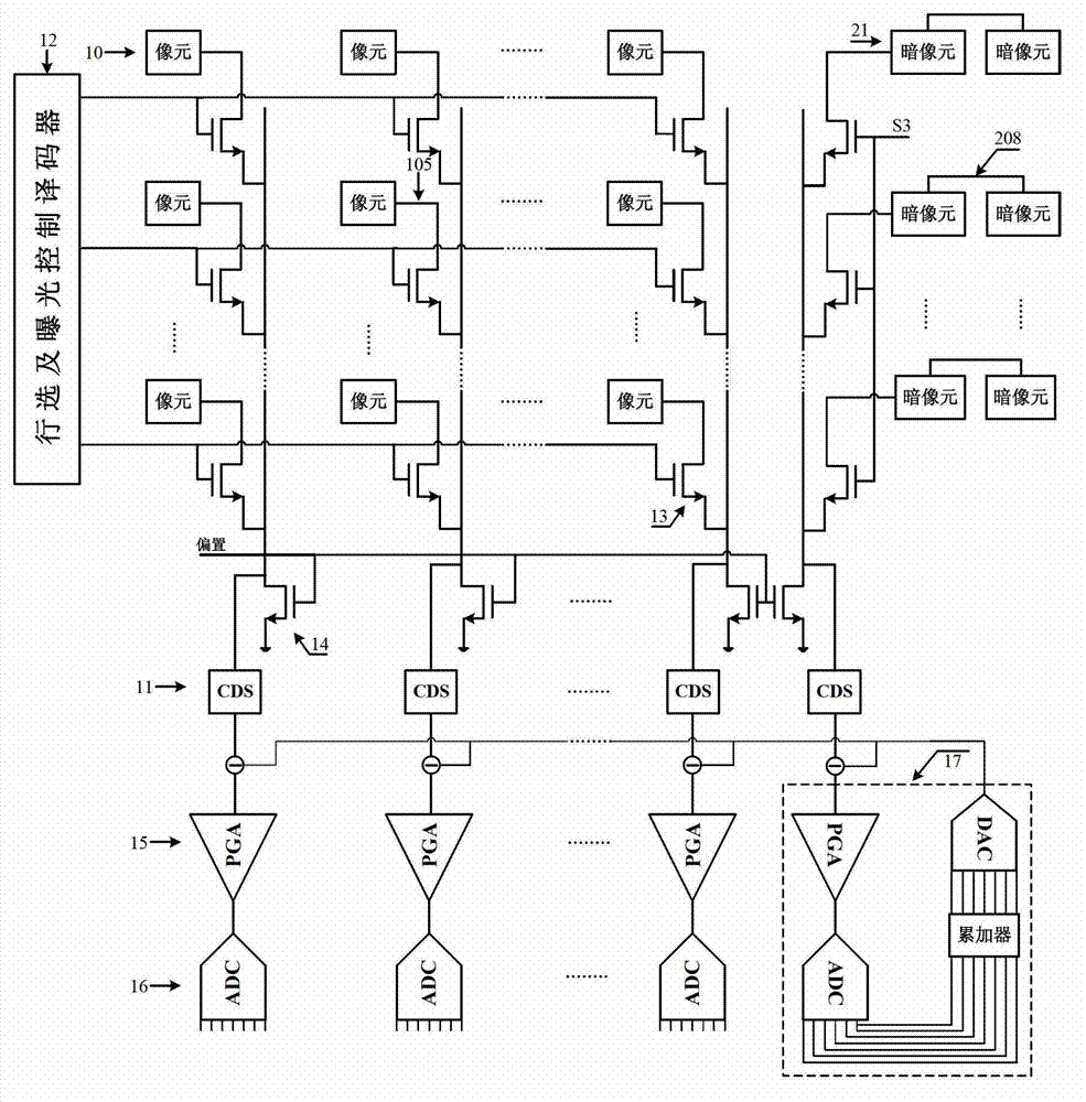
[0044] Such as figure 1 Shown is the overall layout structure of a typical CMOS image sensor, 10 is a photosensitive pixel array, which converts light signals of different intensities into analog electrical signals, and connects them to the column lines through the row selection switch 13, and 11 is the column readout circuit , to quantize the analog electrical signal into a digital signal that is easy to store and transmit.
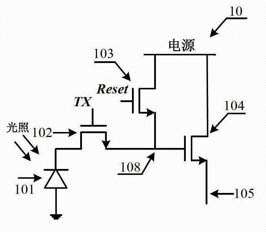
[0045] Such as figure 2It is a single pixel circuit of a pixel array, including a photodiode 101, a transfer tube 102, a reset switch 103, and a source follower input tube 104. Light of different intensities generates different amounts of charges in the photodiode 101, and these charges pass through the transfer tube 102 is transmitted to the FD node 108 to convert t...
PUM
 Abstract
Description
Claims
Application Information
 - R&D
- Intellectual Property
- Life Sciences
- Materials
- Tech Scout
- Unparalleled Data Quality
- Higher Quality Content
- 60% Fewer Hallucinations
Browse by: Latest US Patents, China's latest patents, Technical Efficacy Thesaurus, Application Domain, Technology Topic, Popular Technical Reports.
© 2025 PatSnap. All rights reserved.Legal|Privacy policy|Modern Slavery Act Transparency Statement|Sitemap|About US| Contact US: help@patsnap.com