Supercharge Your Innovation With Domain-Expert AI Agents!

FinFET (field effect transistor) device manufacturing method

A device manufacturing method and substrate technology, applied in semiconductor/solid-state device manufacturing, semiconductor devices, electrical components, etc., can solve the problems of large channel area and cannot meet the requirements of smaller size of FinFET devices, etc., and achieve high drive current , increase the channel stress, improve the effect of driving current

Active Publication Date: 2013-05-29
SEMICON MFG INT (SHANGHAI) CORP +1
View PDF6 Cites 4 Cited by
  • Summary
  • Abstract
  • Description
  • Claims
  • Application Information

AI Technical Summary

Problems solved by technology

However, the channel area produced by this type of method becomes larger, which can no longer meet the requirements for smaller size of FinFET devices at 22nm and below technology nodes

Method used


Image

  • FinFET (field effect transistor) device manufacturing method
  • FinFET (field effect transistor) device manufacturing method
  • FinFET (field effect transistor) device manufacturing method

Examples


Embodiment Construction

[0031] The method for manufacturing a FinFET device proposed by the present invention will be further described in detail below with reference to the accompanying drawings and specific embodiments.

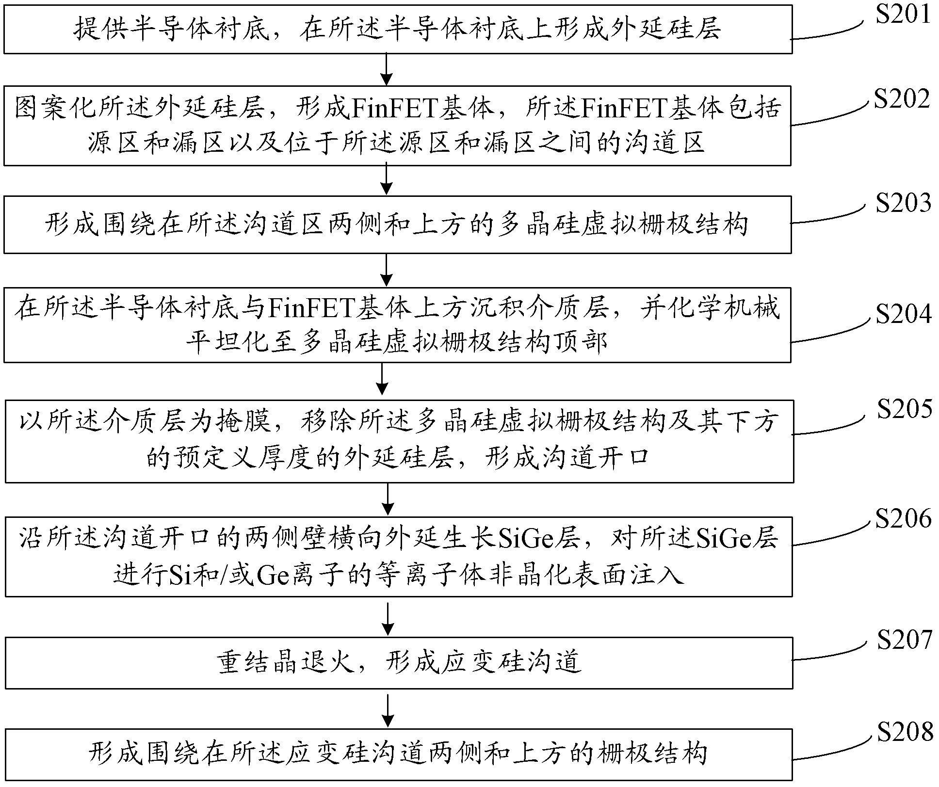
[0032] Such as figure 2 As shown, the present invention proposes a method for manufacturing a FinFET device, comprising:

[0033] S201, providing a semiconductor substrate, and forming an epitaxial silicon layer on the semiconductor substrate;

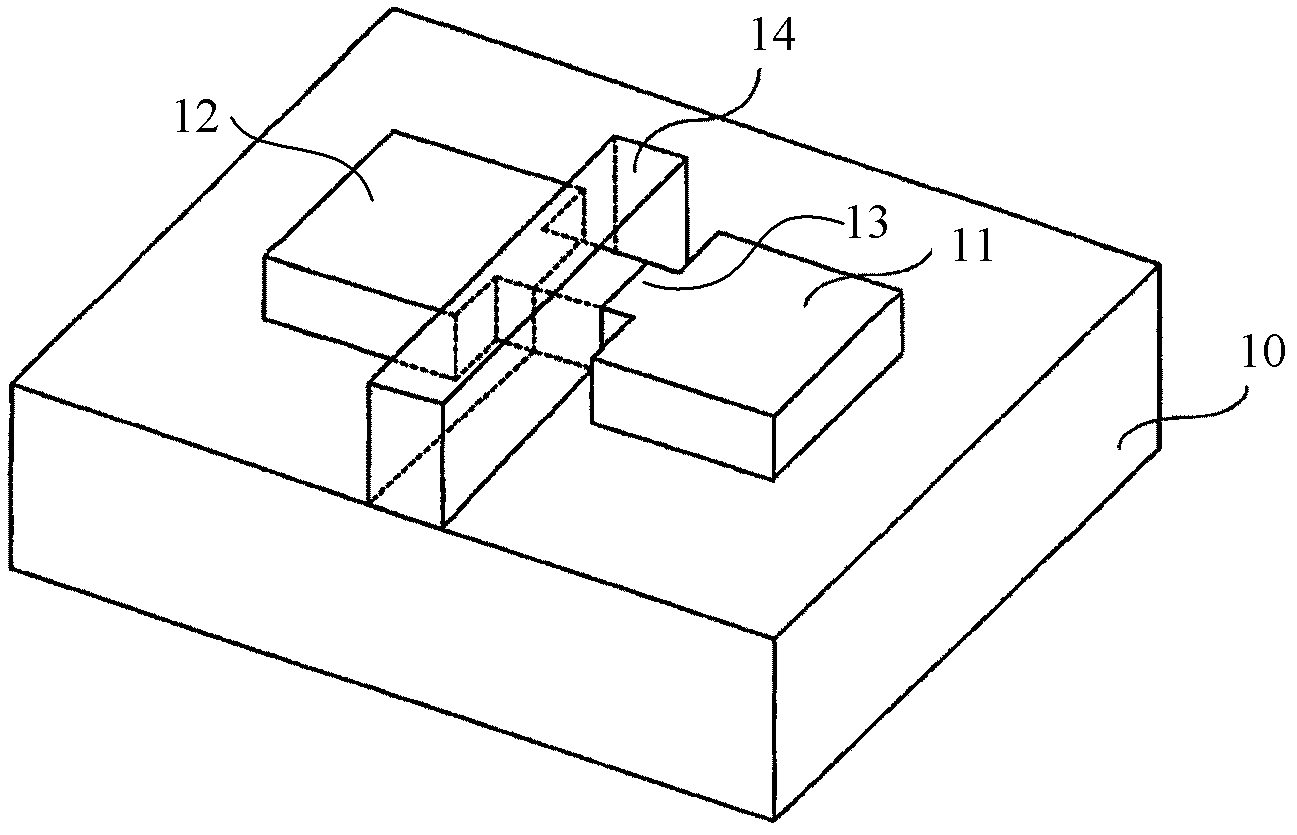
[0034] S202, patterning the epitaxial silicon layer to form a FinFET base, where the FinFET base includes a source region and a drain region and a channel region between the source region and the drain region;

[0035] S203, forming polysilicon dummy gate structures surrounding and above the channel region;

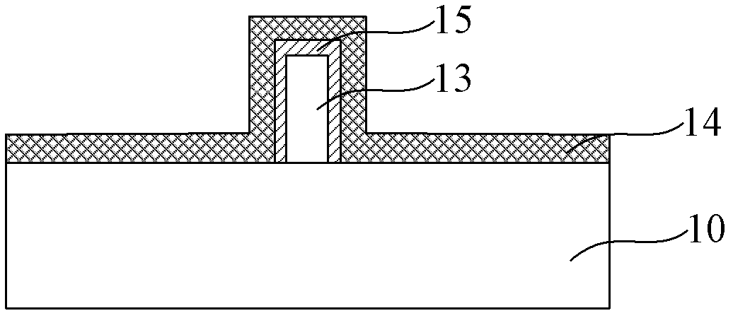
[0036] S204, depositing a dielectric layer on the semiconductor substrate and the FinFET base, and chemically mechanically planarizing to the top of the polysilicon dummy gate structure;

[0037] S205, using the dielectric layer as...


PUM


Abstract

The invention provides an FinFET (field effect transistor) device manufacturing method. The method includes: forming a fin strain germanium-silicon channel at an original position of a fin channel area, so that original width-length ratio and size of the fin channel are maintained, channel stress is increased, and driving current of the FinFET device is improved; and in addition, the hourglass-shaped fin strain germanium-silicon channel is higher than a strip-shaped fin strain germanium-silicon channel in width-length ratio, and the fin strain germanium-silicon channel comprising a strain germanium-silicon layer and a strain carbon-silicon layer is higher in stress performance, so that the obtained FinFET device is higher in driving current.

Description

technical field [0001] The invention relates to the field of semiconductor manufacturing, in particular to a method for manufacturing a FinFET device. Background technique [0002] MOSFET (Metal Oxide Semiconductor Field-Effect Transistor) is the main component of most semiconductor devices. When the channel length is less than 100nm, in the traditional MOSFET, the source and drain regions are separated due to the semiconductor material of the semiconductor substrate surrounding the active region. Interaction, the distance between the drain and the source is also shortened, resulting in a short channel effect, so that the control ability of the gate to the channel becomes worse, and it becomes more and more difficult for the gate voltage to pinch off the channel The larger the , the easier it is for the subthrehhold leakage to occur. [0003] Fin field effect transistor (Fin Field effect transistor, FinFET) is a new metal oxide semiconductor field effect transistor, its str...

Claims


Application Information

Patent Timeline
Patent Type & Authority Applications(China)
IPC IPC(8): H01L21/336H01L21/28
Inventor 赵猛三重野文健
Owner SEMICON MFG INT (SHANGHAI) CORP
Features
  • R&D
  • Intellectual Property
  • Life Sciences
  • Materials
  • Tech Scout
  • Unparalleled Data Quality
  • Higher Quality Content
  • 60% Fewer Hallucinations
Learn More