Array substrate, manufacture method of array substrate and display device

An array substrate and manufacturing method technology, applied in the field of display, can solve the problems of slow development of LTPSTFT technology, difficult competition of amorphous silicon TFT products, and various production processes, so as to reduce the number of patterning processes, shorten production time, and improve product quality Effect

Active Publication Date: 2013-05-29
BOE TECH GRP CO LTD
View PDF5 Cites 33 Cited by
  • Summary
  • Abstract
  • Description
  • Claims
  • Application Information

AI Technical Summary

Problems solved by technology

[0018] The traditional manufacturing process of low-temperature polysilicon thin film transistor (thin film transistor, referred to as TFT) array substrate through 7 mask process (7Mask LTPS TFT) is relatively complicated, and the manufacturing process is complicated, resulting in an increase in its manufacturing cost, which is difficult to compare with amorphous Silicon TFT products compete, making the development of LTPS TFT technology slow

Method used


Image

  • Array substrate, manufacture method of array substrate and display device
  • Array substrate, manufacture method of array substrate and display device
  • Array substrate, manufacture method of array substrate and display device

Examples


Embodiment 1

[0066] Combine below Figure 1 to Figure 9 The manufacturing method of the array substrate in the embodiment of the present invention will be described in detail.

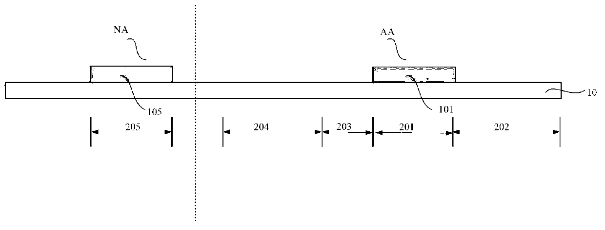
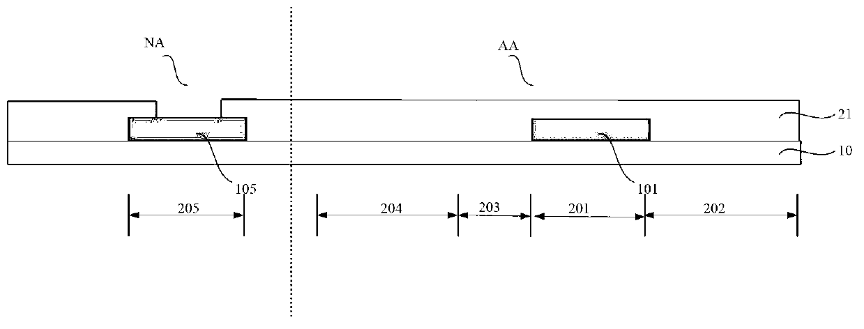
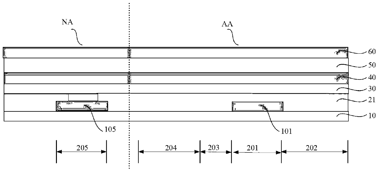
[0067] The manufacturing method of the array substrate in the embodiment of the present invention includes forming a thin film transistor and a pixel electrode pattern on a base substrate. The thin film transistor at least includes a gate electrode pattern, an active layer pattern, a source electrode pattern and a drain electrode pattern,

[0068] Wherein, the source electrode pattern, the drain electrode pattern, the pixel electrode pattern and the active layer pattern are formed in one patterning process through a three-gray-level mask process.

[0069] The source pattern, drain pattern, pixel electrode pattern, and active layer pattern are formed in one patterning process through the three-gray-level mask process, which can reduce the number of times the mask is used, simplify the production process, and greatly reduce ...

Embodiment 2

[0113] In this embodiment, an array substrate is provided, which includes a thin film transistor and a pixel electrode pattern formed on a base substrate. The thin film transistor at least includes a gate electrode pattern, an active layer pattern, a source electrode pattern, and a drain electrode pattern. The source electrode pattern, the drain electrode pattern, the pixel electrode pattern, and the active layer pattern are formed by one patterning process.

[0114] Specifically, the array substrate includes:

[0115] Base substrate

[0116] A pattern including a gate electrode on the base substrate;

[0117] A gate insulating layer pattern located above the pattern including the gate electrode;

[0118] A pattern including an active layer located above the gate insulating layer pattern, the active layer pattern being formed of an active layer thin film formed above the gate insulating layer pattern, the active layer pattern including a source electrode Region, drain region and chann...

Embodiment 3

[0148] This embodiment provides a display device, including the array substrate in the second embodiment. Since the array substrate has the advantages of low cost and high quality, the cost of the display device can be reduced and the quality of the display device can be improved.


PUM


Abstract

The invention belongs to the technical field of display and discloses an array substrate and a manufacture method of the array substrate. Source electrode patterns, drain electrode patterns, pixel electrode patterns and active layer patterns of the array substrate are formed through the once picture composition process. Compared with the traditional manufacture process of the array substrate, the manufacture method of the array substrate is simple in process, shortens production time, reduces product cost and improves product quality.

Description

Technical field [0001] The present invention relates to the field of display technology, in particular to an array substrate, a manufacturing method thereof, and a display device. Background technique [0002] Thin Film Transistor (TFT) can be divided into poly-Si (P-Si) TFT and amorphous silicon (a-Si) TFT. The difference between the two lies in the characteristics of the transistor. Due to the inherent defects of amorphous silicon a-Si, such as low on-state current, low mobility and poor stability caused by many defect states, it is restricted in many fields. The arrangement of the molecular structure of P-Si in a grain is neat and directional, so the electron movement rate is 200-300 times faster than that of disordered amorphous silicon. P-Si products mainly include high-temperature poly-silicon (HTPS) and low-temperature poly-silicon (LTPS). [0003] LTPS technology is a new generation of TFT display manufacturing process, mainly through excimer laser annealing (ELA), metal ...

Claims


Application Information

Patent Timeline
Patent Type & Authority Applications(China)
IPC IPC(8): H01L21/77H01L27/12
CPCH01L29/6675H01L2227/323H01L27/1288H01L27/124H01L29/786H10K59/1201
Inventor 马占洁
Owner BOE TECH GRP CO LTD
Why Eureka
Try Eureka