Package substrate of active chip and preparation method thereof

A technology of active chips and packaging substrates, which is applied to printed circuits connected to non-printed electrical components, semiconductor/solid-state device manufacturing, semiconductor/solid-state device components, etc., can solve the problem of reducing the size of the package body and packaging Large structure and other problems, to achieve the effect of integrated production, improve production efficiency and simplify the production process

Active Publication Date: 2013-06-05
NAT CENT FOR ADVANCED PACKAGING
View PDF6 Cites 13 Cited by
  • Summary
  • Abstract
  • Description
  • Claims
  • Application Information

AI Technical Summary

Problems solved by technology

[0006] U.S. Patent No.7663249B2 proposes a chip packaging structure and manufacturing method, such as Figure 1B As shown, in this method, the packaged chips 108 and 208 are respectively connected to two substrates by flip-chip welding technology, and a layer of dielectric layer 120 is first laminated on a substrate connected to the packaged chip 108, and then another The substrate that has been flip-chip connected to the packaged chip 208 is pressed face down to the dielectric layer 120, and then the substrates on both sides are removed, thus realizing the embedding of multiple packaged chips, but in the above-mentioned patent, the chips are flip-chip connected to the substrate Then press the dielectric layer, so when there are many bumps and the spacing is relatively small, it is possible that the dielectric layer cannot completely fill the gap between the bumps of the chip and the bumps (ie Figure 1B In B), the existence of bubbles is caused, and the chip has been packaged, so the size of the chip itself is very large, and the package structure will be relatively large, so it is difficult to reduce the size of the entire package

Method used


Image

  • Package substrate of active chip and preparation method thereof
  • Package substrate of active chip and preparation method thereof
  • Package substrate of active chip and preparation method thereof

Examples


Embodiment Construction

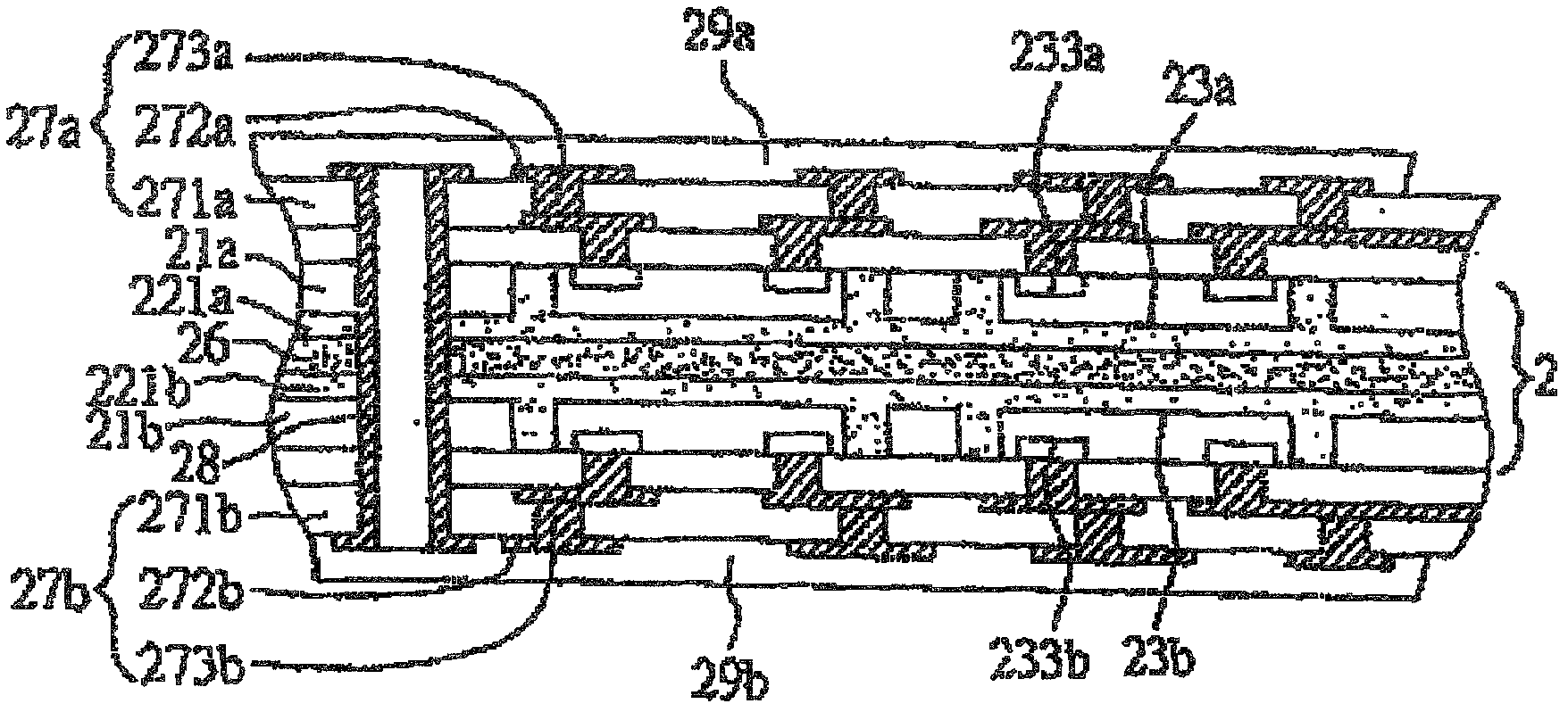
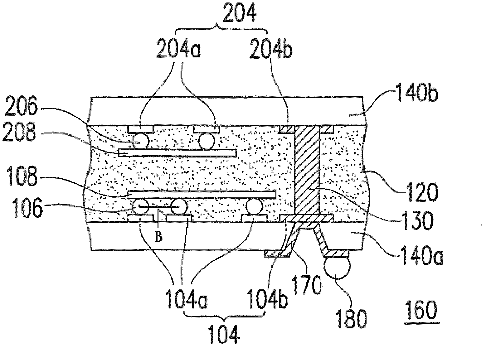
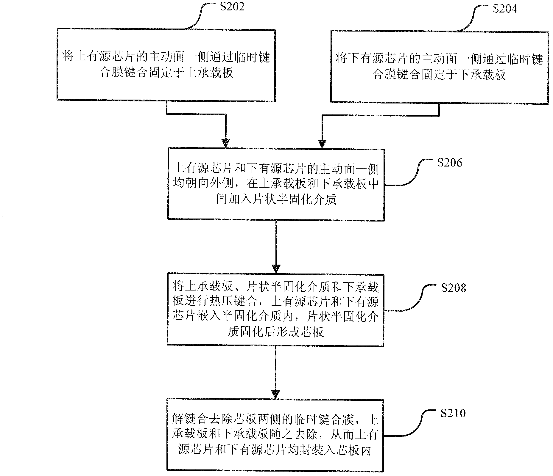
[0045]In order to make the object, technical solution and advantages of the present invention clearer, the present invention will be described in further detail below in conjunction with specific embodiments and with reference to the accompanying drawings. It should be noted that while examples of parameters including particular values ​​may be provided herein, it should be understood that the parameters need not be exactly equal to the corresponding values, but rather may approximate the values ​​within acceptable error margins or design constraints. For ease of description, at first the various components involved in the present invention are numbered:

[0046] 100-on the active chip; 101-on the metal electrode of the active chip;

[0047] 102-the first passivation layer on the active chip, with openings to expose the electrodes;

[0048] 103 - the second passivation layer on the active chip;

[0049] 104 - temporary bonding film;

[0050] 105-upper bearing plate;

[005...


PUM


Abstract

The invention provides a package substrate of an active chip and a preparation method of the package substrate of the active chip. The package substrate of the active chip comprises a core plate. The core plate comprises at least one upper active chip, and at least one lower active chip. The upper active chip is embedded into the core plate, an active face faces toward the lower surface of the core plate, and the upper active chip is an active unpacked chip. The lower active chip is embedded into the core plate, an active face faces toward the upper surface of the core plate and the lower active chip is an active unpacked chip. Due to the fact that the active chips are not packed before being embedded, thinning processing is carried out on the active chips, so that microminiaturization and light weight of the package structure are achieved, and therefore the manufacturing technology of the substrate is simplified. In addition, a plurality of the unpacked chips are simultaneously embedded into two faces of the substrate, and integrality is improved. Meanwhile, the freedom degree and the space on the two faces of the substrate are large, multi-layer wiring can be continuously carried out, and therefore process quality and reliability of electrical connection are improved.

Description

technical field [0001] The invention relates to the technical field of system packaging in the microelectronics industry, in particular to an active chip packaging substrate and a method for preparing the substrate. Background technique [0002] Modern portable electronic products put forward higher requirements for microelectronic packaging. With the continuous pursuit of lighter, thinner, smaller, high reliability and low power consumption, microelectronic packaging is also moving towards higher density and smaller size. Small package form development. Microelectronic packaging will develop from packaging, less packaging to no packaging, so Direct Chip Attach (DCA) technology has attracted more and more attention. Direct chip bonding technology is a packaging technology with the highest packaging efficiency. It directly bonds the chip to the printed circuit board or substrate without packaging. The advantage is that it has better electrical properties and more direct heat...

Claims


Application Information

Patent Timeline
IPC IPC(8): H01L25/065H01L21/98H01L23/31H01L23/538H01L21/56H05K1/18
CPCH01L24/96H01L21/568H01L2224/04105H01L2224/19H01L2224/24H01L2224/92144H01L2924/00012
Inventor 于中尧张霞
Owner NAT CENT FOR ADVANCED PACKAGING
Why Eureka
Try Eureka