Pixel structure for improving charge transfer efficiency and reducing dark current and working method of pixel structure

A technology of charge transfer efficiency and pixel structure, which is applied to color TV components, TV system components, TVs, etc., can solve problems affecting electron transfer efficiency and image smearing, so as to improve charge transfer efficiency and reduce Dark current, reducing the effect of image smearing

Inactive Publication Date: 2013-06-12
TIANJIN UNIV
View PDF4 Cites 16 Cited by
  • Summary
  • Abstract
  • Description
  • Claims
  • Application Information

AI Technical Summary

Problems solved by technology

However, due to the flat potential under the transfer gate, after the charge transfer is completed, the remaining electrons in the channel may flow

Method used


Image

  • Pixel structure for improving charge transfer efficiency and reducing dark current and working method of pixel structure
  • Pixel structure for improving charge transfer efficiency and reducing dark current and working method of pixel structure
  • Pixel structure for improving charge transfer efficiency and reducing dark current and working method of pixel structure

Examples


Embodiment Construction

[0022] The pixel structure for improving charge transfer efficiency and reducing dark current and its working method of the present invention will be described in detail below in conjunction with the embodiments and the accompanying drawings.

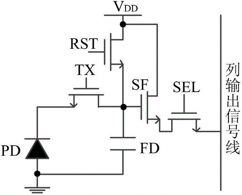
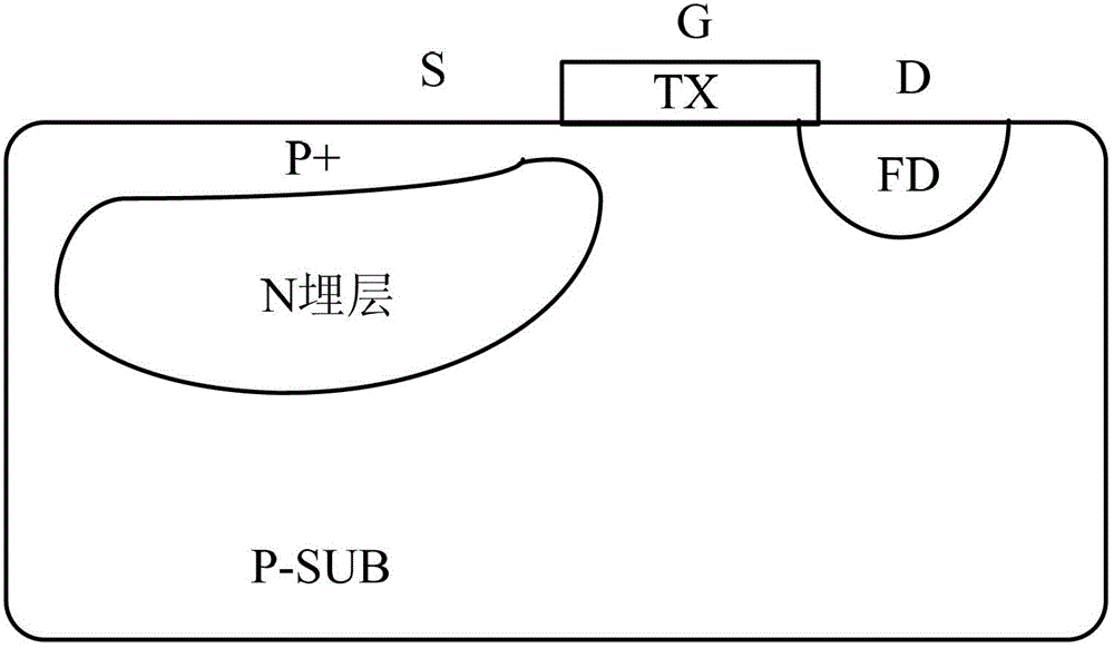
[0023] As shown in Fig. 4(a) and Fig. 5(a), the pixel structure of the present invention improves the charge transfer efficiency and reduces the dark current. On the basis of the traditional 4T active pixel, the gate structure of the transmission tube (TX) is changed. It includes a reset transistor RST, a transfer transistor TX, a selection transistor SEL, a source follower transistor SF, a photodiode PD and a floating diffusion region FD, wherein the N terminal of the photodiode PD is connected to the source of the transfer transistor TX, and the photodiode PD The P terminal is grounded, the drain of the transmission transistor TX, the source of the reset transistor RST, the gate of the source follower transistor SF and one end of the f...


PUM


Abstract

The invention relates to a pixel structure for improving a charge transfer efficiency and reducing dark current and a working method of the pixel structure. An N end of a photoelectric diode PD is connected with a source electrode of a transmission transistor TX, a P end of the photoelectric diode PD is grounded, a drain electrode of the transmission transistor TX, a source electrode of a resetting transistor RST, a grid electrode of a source tracking transistor SF and one end of a floating dispersion area FD are connected together, the other end of the floating dispersion area FD is grounded, a drain electrode of the resetting transistor RST and a drain electrode of the source tracking transistor SF are connected with a power supply VDD, a source electrode of the source tracking transistor SF is connected with a drain electrode of a selection transistor SEL, a source electrode of the selection transistor SEL is an output end which is connected to a column output signal wire, and a grid electrode of the transmission transistor TX is divided into a first grid electrode TX1 and a second grid electrode TX2. A dual-grid structure is adopted on a transmission pipe, and the dark current is reduced by applying different bias voltage in a charge integrating and charge transferring process, so that the well capacity is increased, the potential distribution in a charge transfer route is optimized, the charge transfer can be better facilitated, and the image streaking can be reduced.

Description

technical field [0001] The invention relates to a pixel structure. In particular, it relates to a pixel structure for improving charge transfer efficiency and reducing dark current and a working method thereof. Background technique [0002] Although CCD (Charge Couple Device, CCD) is widely used in image sensors, CMOS image sensors (CMOS Image Sensors, CIS) are widely used in digital cameras, scanning equipment, etc. due to its advantages of low power consumption, easy integration and low cost. Very attractive in application. Due to the high power consumption of the traditional CCD image sensor and the incompatibility with the standard CMOS process, which increases the cost, it is gradually being replaced by the rapidly developing CMOS image sensor. [0003] The pixel array in a CMOS image sensor is the part that collects light signals and converts them into electrical signals, which has an important impact on the performance of the image sensor. The existing pixel struct...

Claims


Application Information

Patent Timeline
IPC IPC(8): H04N5/361H04N5/378H01L27/146
Inventor 姚素英张冬苓徐江涛史再峰高静高志远
Owner TIANJIN UNIV
Why Eureka
Try Eureka