
Programming method for multi-bit nonvolatile memory cell and multi-bit nonvolatile memory unit array

A technology of non-volatile storage and programming method, which is applied in the field of programming p-type channel multi-bit non-volatile memory cells and arrays, and can solve the problem that p-type channel multi-bit non-volatile memory cells cannot take into account programming speed and programming accuracy, etc. problems, to achieve the effect of increasing programming speed, improving programming accuracy, and taking into account both programming speed and accuracy

Inactive Publication Date: 2013-06-19
INST OF MICROELECTRONICS CHINESE ACAD OF SCI
View PDF3 Cites 2 Cited by
  • Summary
  • Abstract
  • Description
  • Claims
  • Application Information

AI Technical Summary

Problems solved by technology

[0005] The main purpose of the present invention is to solve the problem that the traditional programming method cannot take into account both programming speed and programming accuracy when programming p-type channel multi-bit non-volatile memory cells

Method used

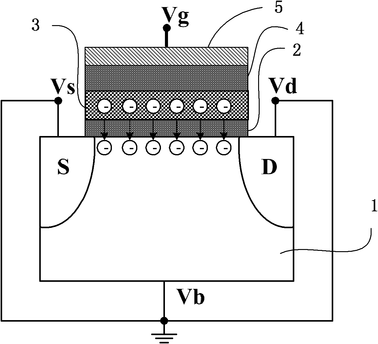
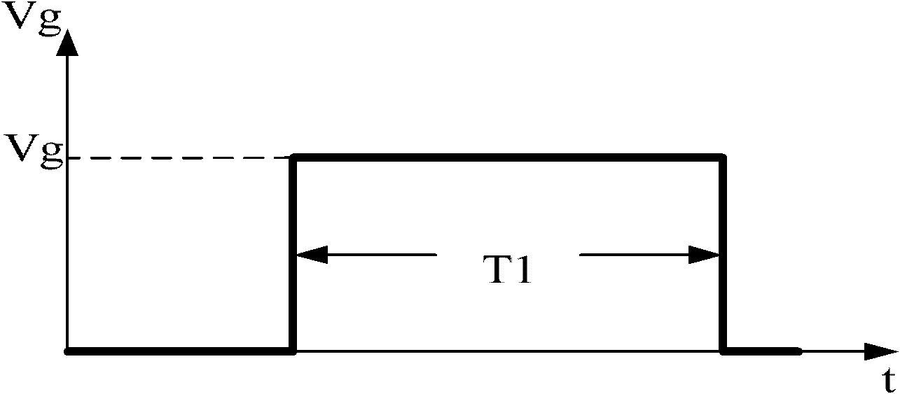
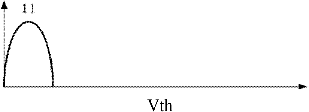

Image

  • Programming method for multi-bit nonvolatile memory cell and multi-bit nonvolatile memory unit array
  • Programming method for multi-bit nonvolatile memory cell and multi-bit nonvolatile memory unit array
  • Programming method for multi-bit nonvolatile memory cell and multi-bit nonvolatile memory unit array

Examples


Embodiment Construction

[0023] When the traditional programming method is used to program p-type channel multi-bit non-volatile memory cells, verification must be performed after each programming. If the required state is not programmed, it is necessary to increase the number of programming times and repeat verification until the required state is programmed. The threshold voltage of memory cells will increase after each programming. To make the threshold voltages of all memory cells distributed in a narrow range after programming, the pulse amplitude applied during programming should be low, so that after each programming, memory The increase of the threshold voltage of the cell is small, but this will significantly increase the number of programming times for a single cell, thereby greatly increasing the programming time of the memory cell; if you want to speed up the programming speed of the memory cell and reduce the programming time, you need to apply a larger magnitude during programming. Pulse,...


PUM


Abstract

The invention provides a programming method for a multi-bit nonvolatile memory cell. The programming method comprises the steps of applying identical positive bias voltages on a substrate and a source terminal of a p-channel non-volatile memory cell, with a drain terminal grounded, applying a programming pulse voltage on a grid electrode; and programming the multi-bit nonvolatile memory cell in a setting state after a plurality of programming cycles comprising an electronic FN tunneling process and a channel hot electron injection process. Accordingly, the invention provides a programming method for a multi-bit nonvolatile memory unit array. A process for forming a memory cell threshold voltage steady state of the programming method provided by the invention is a self-convergence process and a repeated inspection process of a conventional programming method is omitted, so that programming speed of the multi-bit nonvolatile memory is effectively increased. By setting pulse parameters for the FN tunneling process and the channel hot electron injection process, the memory cell can be directly programmed to a designated state, so that programming accuracy of the multi-bit non-volatile memory cell is increased, and programming speed and accuracy can be taken into account at the same time.

Description

technical field [0001] The invention relates to the technical field of semiconductor memory, in particular to a method for programming p-type channel multi-bit non-volatile memory cells and arrays. Background technique [0002] At present, the development of memory technology has become an important driving force for the advancement of integrated circuit design and manufacturing, and occupies a very important position in the field of microelectronics. While the storage device structure is developing towards nanometer feature size, it is facing severe challenges in terms of storage speed and density. Multi-bit non-volatile storage technology can generate multi-level storage states, effectively improving the storage density of the memory. [0003] Non-volatile memory cell structure see figure 1 , including an n-type silicon substrate 1, a p-type heavily doped source region S and a drain region D on the silicon substrate, a tunneling dielectric layer 2 covering the carrier cha...

Claims


Application Information

Patent Timeline
Patent Type & Authority Applications(China)
IPC IPC(8): G11C16/34G11C16/02
Inventor 刘明姜丹丹霍宗亮张满红刘璟谢常青
Owner INST OF MICROELECTRONICS CHINESE ACAD OF SCI
Learn More