
Method for detecting load effect of grinding process

A technology of load effect and grinding process, applied in grinding devices, grinding machine tools, manufacturing tools, etc., can solve the problems of excessive grinding, different, undisclosed grinding rates, etc., to improve product performance, avoid load effects, and increase yield. Effect

Active Publication Date: 2013-06-26
SHANGHAI HUALI MICROELECTRONICS CORP
View PDF8 Cites 3 Cited by
  • Summary
  • Abstract
  • Description
  • Claims
  • Application Information

AI Technical Summary

Problems solved by technology

This technical document also does not disclose any relevant technical features related to solving the problem of excessive grinding defects caused by different grinding rates caused by different pattern densities

Method used


Image

  • Method for detecting load effect of grinding process
  • Method for detecting load effect of grinding process

Examples


Embodiment Construction

[0028] The specific embodiment of the present invention will be further described below in conjunction with accompanying drawing:

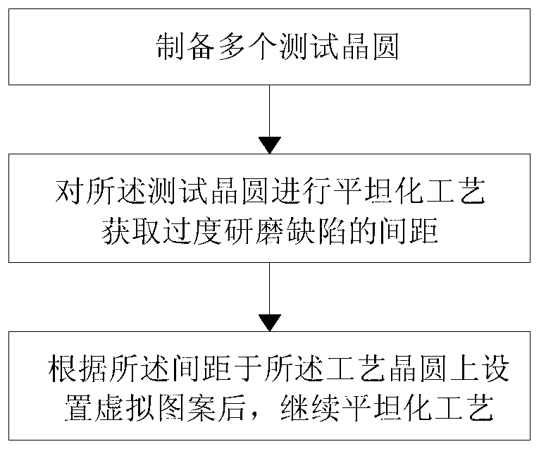
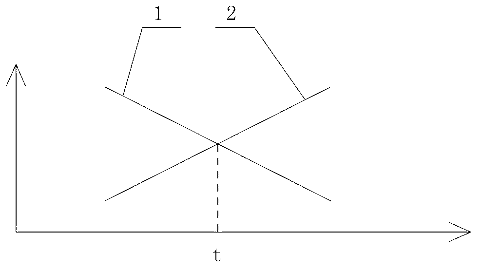
[0029] figure 1 It is a schematic flow diagram of the method for detecting the grinding process load effect in the embodiment; figure 2 It is a schematic diagram of the functional relationship between the planarization process time and the overgrinding defect and the remaining oxide in the embodiment, wherein the horizontal axis represents the process time value, the vertical axis represents the overgrinding defect value and the remaining oxide value, and the straight line 1 represents the process The functional relationship between the time and the remaining oxide, the straight line 2 represents the functional relationship between the process time and the overgrinding defect, and the time t is the optimal process time value of the planarization process. Such as Figure 1-2 As shown, a method for detecting the load effect of the grinding proces...


PUM


Abstract

The invention relates to the field of semiconductor fabrication, in particular to a method for detecting a load effect of a grinding process. A test wafer is adopted to test a grinding defect spacing of a planarization process and optimal process time of the grinding process, virtual patterns corresponding to the spacing are arranged on a process wafer, a planarization process of the optimal process time is carried out on the process wafer, and therefore generation of the load effect caused by different densities of pictures on the wafers can be effectively avoided, the product performance is improved, and meanwhile the product yield is increased.

Description

technical field [0001] The invention relates to the field of semiconductor manufacturing, in particular to a method for detecting the load effect of a grinding process. Background technique [0002] With the development of integrated circuit technology and the improvement of integration, the virtual graphics area on the edge of the chip on the wafer is often used to lay out some functional circuits. Because these areas are close to the chip dicing line, they often have a relatively empty area, while in The process operation in actual production can easily form different process conditions in the open area and dense area of ​​the wafer, resulting in a load effect, especially when the planarization process is performed on a large-sized wafer, the formed load effect is more obvious; for example, in When the chemical mechanical polishing process (CMP) is performed on the wafer, since the entire wafer is ground together, the large-sized wafer (such as a wafer with a diameter of 3...

Claims


Application Information

Patent Timeline
Patent Type & Authority Applications(China)
IPC IPC(8): B24B37/04B24B37/013
Inventor 龙吟范荣伟王洲男倪棋梁王恺陈宏璘
Owner SHANGHAI HUALI MICROELECTRONICS CORP
Learn More