
Optical proximity correction method, connection hole manufacturing method

A technology of optical proximity correction and manufacturing method, which is applied in the direction of optics, pattern surface photolithography, and originals for photomechanical processing. Effect

Active Publication Date: 2016-10-05
SEMICON MFG INT (SHANGHAI) CORP
View PDF6 Cites 0 Cited by
  • Summary
  • Abstract
  • Description
  • Claims
  • Application Information

AI Technical Summary

Problems solved by technology

Because the layout style of the original layout graphics varies with the designer and has diversity, directly performing optical proximity correction on the original layout graphics will usually obtain a large number of patterns to be marked and corrected, so that the correction process will take a lot of manpower and time

Method used


Image

  • Optical proximity correction method, connection hole manufacturing method
  • Optical proximity correction method, connection hole manufacturing method
  • Optical proximity correction method, connection hole manufacturing method

Examples


Embodiment 1

[0075] Input customer's original layout data in OPC software, including V 1 layers and M 2 ADI target for each graph of the layer.

[0076] The process window of the lithography process includes two aspects: the depth of focus DOF ​​and the exposure energy range, each of which has a tolerable error range, and the combined error range of the two aspects is the process window of the lithography process. to V 1 Continuously do about 10 iterations of OPC correction and simulation cycles to find graphics with a small process window; sort and classify these weak graphics themselves and the characteristics of the surrounding environment to form a weak graphics library;

[0077] Compare these positions with M 2 Compared with the target layer of the layer, check its connection relationship, if a certain V is found 1 V 1 The ADI of the layer increases;

[0078] In one embodiment, calling out V 1 layers and M 2 Layer mask layout information, compare the coordinate information of ...


PUM


Abstract

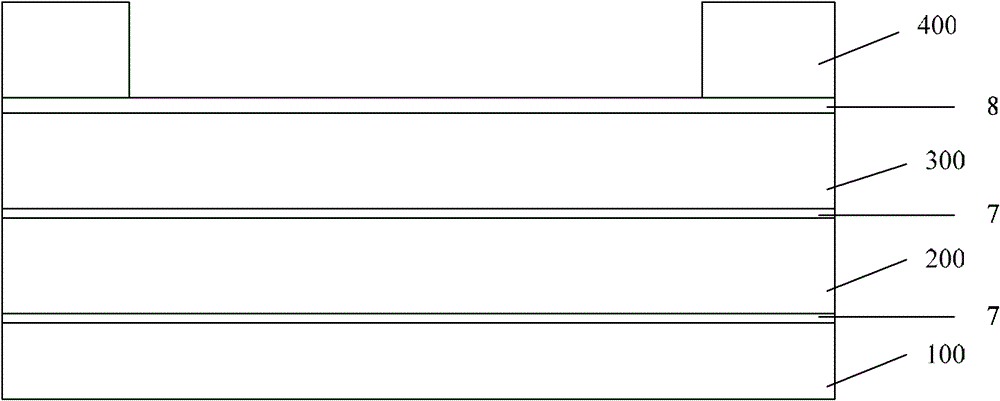
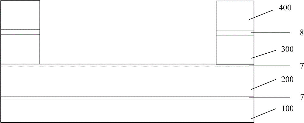
The invention discloses an optical proximity correction method applied in manufacture process of a semiconductor structure, and a manufacture method of connecting holes. According to the optical proximity correction method, the semiconductor structure at least includes an upper layer and a lower layer, and the photolithography technique is used for defining multiple through holes in the lower layer. The optical proximity correction method includes the following steps: comparing the layout of the upper layer and the layout of the lower layer, and finding out the boundary, proximate to the border of a notch, of a through hole; if one boundary of a certain through hole is proximate to the border of the notch, performing amplification correction on an ADI value of the lower layer in the direction of the boundary; and performing OPC (optical proximity correction) on the lower layer by utilizing the corrected ADI value, so as to form a mask plate of the lower layer. According to the methods, the relationship that the boundaries of certain through holes are aligned to the boundary of an interconnection slot of the previous layer in the damascene process is utilized, and special optical proximity correction is performed on the boundaries of the through holes aligned to the boundary of the interconnection slot, so that the effect of increasing photolithography technique windows at the boundaries of the through holes is achieved.

Description

technical field [0001] The invention relates to the field of semiconductor manufacturing, in particular to semiconductor lithography technology and optical proximity effect correction technology. Background technique [0002] In the semiconductor manufacturing process, the photolithography process plays a central role and is the most important process step in the production of integrated circuits. [0003] With the development of semiconductor manufacturing technology, the feature size is getting smaller and smaller, and the requirements for resolution in photolithography technology are getting higher and higher. Photolithography resolution refers to the minimum feature size (Critical Dimension, CD) that can be exposed on the surface of a silicon wafer by a photolithography machine, and is one of the important performance indicators in photolithography technology. The resolution of the exposure machine will have an impact on the final size and density of the IC circuit. Th...

Claims


Application Information

Patent Timeline
Patent Type & Authority Patents(China)
IPC IPC(8): G03F1/36H01L21/60
Inventor 张婉娟林益世
Owner SEMICON MFG INT (SHANGHAI) CORP
Learn More