
Method of manufacturing mask read-only memory

A mask read-only, manufacturing method technology, applied in semiconductor/solid-state device manufacturing, electrical solid-state devices, semiconductor devices, etc., can solve problems such as memory unit failure, small photolithography process window, island pattern drift, etc.

Inactive Publication Date: 2014-10-15
SHANGHAI HUAHONG GRACE SEMICON MFG CORP
View PDF9 Cites 0 Cited by
  • Summary
  • Abstract
  • Description
  • Claims
  • Application Information

AI Technical Summary

Problems solved by technology

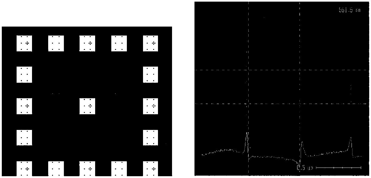
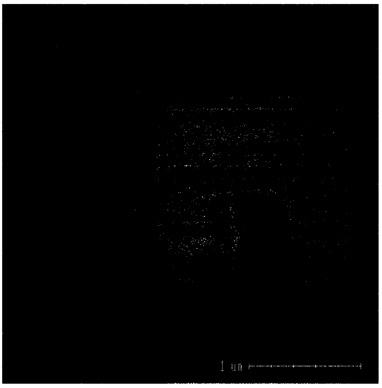
in, figure 1 In the actual process control of the island structure shown, the photolithography process window is very small, and the phenomenon of island pattern drift (such as image 3 As shown), the place that does not need ion implantation will be implanted, and the place that needs to be implanted may be blocked by the drifting island pattern, so that the entire memory cell will fail
At present, the analysis reason is mainly because the island pattern is formed on the gate, the island pattern protrudes from both sides of the gate, and the gap between the gates is in a suspended state, such as Figure 4 shown, prone to tilting

Method used


Image

  • Method of manufacturing mask read-only memory
  • Method of manufacturing mask read-only memory
  • Method of manufacturing mask read-only memory

Examples


Embodiment Construction

[0033] A mask read-only memory manufacturing method according to the present invention comprises the following steps:

[0034] In the first step, an active region and an isolation region are formed on the silicon substrate 1 .

[0035] Step 2, forming gate oxide layer 2 and gate 3 of each memory cell transistor of the memory in the active region, such as Figure 5 shown.

[0036] Step 3, implanting to form a source region and a drain region.

[0037] Step 4, make the side wall 4 forming the gate, such as Image 6 shown. This step is an optional step, which can be implemented according to the specific requirements of the product, making or omitting the gate spacer.

[0038] Step 5, depositing the first interlayer dielectric 7, such as Figure 7 shown. The material of the deposited first interlayer dielectric 7 is one or any combination of silicon oxynitride, impurity-free silicate glass, and borophosphosilicate glass. The total thickness of the deposited dielectric materi...


PUM


Abstract

The present invention discloses a method of manufacturing a mask read-only memory. After a grid and a side wall of the grid are finished, a layer of interlayer medium is deposited and flattened, so that a later made island type pattern stands on the grid more firmly. The photoetching process windows are increased, and a deposited medium layer adapts a part of or the whole contacting hole medium layer without needing additional growth or removing, thereby not increasing the manufacture cost additionally.

Description

technical field [0001] The invention relates to the field of semiconductor integrated circuit manufacturing, in particular to a mask read-only memory manufacturing method. Background technique [0002] Mask Read Only Memory (MROM: Mask Read Only Memory) is the most basic read-only memory, widely used in electronic products. The mask read-only memory uses a photomask to selectively implant ions into a plurality of coding regions, so as to determine the connection state of each transistor in the memory cell array, and achieve the purpose of storing data. When the product changes, there is no need to make major changes to the production process, just replace the photomask, which is very conducive to mass production. Compared with EEPROM or Flash, mask read-only memory occupies a very small area, which is beneficial to reduce costs and realize large-capacity storage. [0003] The manufacturing process of the existing mask read-only memory mainly includes the following steps: t...

Claims


Application Information

Patent Timeline
Patent Type & Authority Applications(China)
IPC IPC(8): H01L21/8246H10B20/00
CPCH10B20/363
Inventor 苏波张可钢陈广龙陈华伦朱东园
Owner SHANGHAI HUAHONG GRACE SEMICON MFG CORP
Learn More