Micro heating device

A technology of micro-heating and heating structure, which is applied in the direction of electrical components, electric solid devices, circuits, etc., can solve the problems of unusable, inaccurate control of temperature, inability to accurately determine the magnitude of the current that generates heat, etc., to achieve uniform heating effect

Active Publication Date: 2013-07-03
SEMICON MFG INT (SHANGHAI) CORP
View PDF6 Cites 3 Cited by
  • Summary
  • Abstract
  • Description
  • Claims
  • Application Information

AI Technical Summary

Problems solved by technology

Part of the current applied to the interconnection wire electromigration test device is used to generate Joule electric heat, and the other part is used to test the failure time of the interconnection wire, and the two parts of the current are supplied by the same power source, so it cannot be accurately determined for the interconnection The magnitude of the current used to generate heat during the measurement of the failure time of the wire, so that the temperature applied to the electromigration test device of the interconnection wire cannot be accurately controlled, and the failure time of the electromigration of the interconnection wire under different temperatures cannot be accurately deduced by using the device , leading to inaccurate evaluation of interconnect electromigration

Method used


Image

  • Micro heating device
  • Micro heating device
  • Micro heating device

Examples


no. 1 example

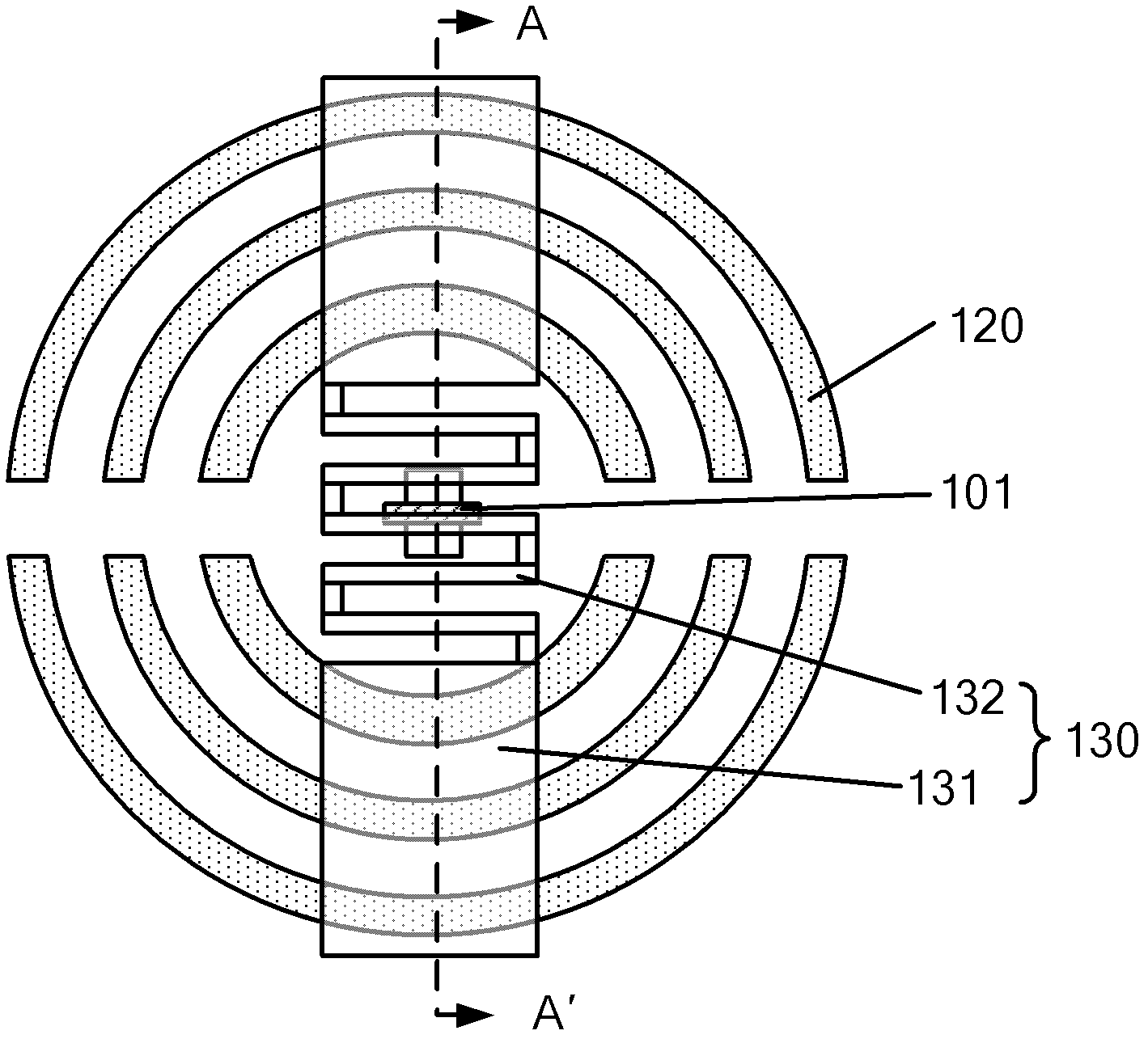
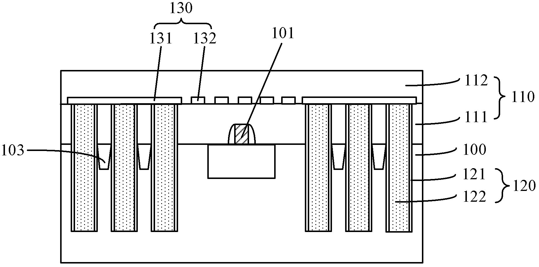
[0034] The first embodiment of the present invention provides a micro heating device, please refer to figure 2 with image 3 , figure 2 It is a structural schematic diagram of a micro-heating device according to an embodiment of the present invention in a top view, image 3 for figure 2 The cross-sectional schematic diagram of the micro-heating device on the line AA' in the middle, specifically including: a semiconductor substrate 100, a device to be tested 101 located on the semiconductor substrate 100; a first interlayer dielectric layer located on the surface of the semiconductor substrate 100 111, a thermal conduction trench 120 located in the semiconductor substrate 100 and the first interlayer dielectric layer 111, the thermal conduction trench 120 is arranged around the device to be tested 101; located on the surface of the first interlayer dielectric layer 111 The heating structure 130, the heating structure 130 includes a heat conduction portion 131 located on t...

no. 2 example

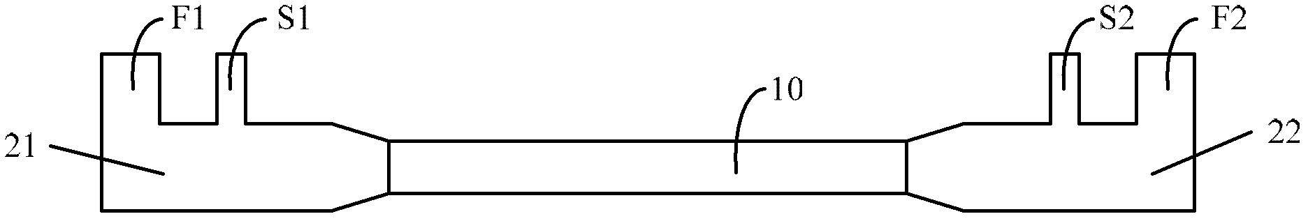
[0045] In the second embodiment of the present invention, please refer to Figure 4 , the structure of the micro-heating device is substantially the same as that of the micro-heating device in the first embodiment, the only difference is that the pattern of the heat conduction groove 120' is a disconnected spiral, and the disconnected spiral A heat conduction groove 120 ′ is arranged around the structure to be inspected 101 , and the structure to be inspected 101 is located at the center of the disconnected spiral heat conduction groove 120 ′, so that the device to be inspected 101 is evenly heated. The spiral shape is a circular spiral or a rectangular spiral, wherein, Figure 4 The pattern of the heat conduction groove 120 ′ is a circular spiral. Since the entire spiral heat conduction groove 120' is divided into two electrically isolated parts, each part is connected to a heat conduction part 131, so that the heating part 132 between the two heat conduction parts 131 gener...

no. 3 example

[0047] Please also refer to Figure 5 with Image 6 , Figure 5 It is a structural schematic diagram of the micro-heating device according to the third embodiment of the present invention in a top view, Image 6 for Figure 5 Schematic diagram of the cross-sectional structure of the micro-heating device on the line BB', specifically including: a semiconductor substrate 100, a device to be tested 101 located on the semiconductor substrate 100; a first interlayer dielectric layer located on the surface of the semiconductor substrate 100 111, a concentric annular thermal conduction trench 120″ located in the semiconductor substrate 100 and the first interlayer dielectric layer 111, the concentric annular thermal conduction trench 120″ is arranged around the device to be tested 101, and The concentric annular heat conduction groove 120" is divided into four electrically isolated parts, and the surface of each part of the heat conduction groove 120" is connected to a different h...


PUM


Abstract

The invention discloses a micro heating device which comprises a semiconductor substrate, a device to be detected that is located on the semiconductor substrate, an interlayer dielectric layer located on the surface of the semiconductor substrate, heat conduction grooves located in the semiconductor substrate and the interlayer dielectric layer, and heating structures located in the interlayer dielectric layer, wherein the heat conduction grooves surround the device to be detected; the heating structures are connected with the heat conduction grooves, and generate heat and conduct the heat into the heat conduction grooves; and the heat conduction grooves are utilized to heat the device to be detected. The heat conduction grooves surround the device to be detected, so that the device to be detected is heated uniformly, and temperature of the device to be detected is controlled by changing the heat generated by the heating structures and controlling the heat generated by the heat conduction grooves.

Description

technical field [0001] The invention relates to semiconductor manufacturing technology, in particular to a micro-heating device for heating up a device to be detected. Background technique [0002] As the integration level of integrated circuits continues to increase, the device density and current rate in integrated circuits become higher and higher, and integrated circuits will generate higher and higher energy. Therefore, high-temperature reliability of devices in integrated circuits is becoming more and more important, and more and more tests on integrated circuits need to be performed at higher temperatures. For example, the electromigration detection of metal interconnection, the time-dependent dielectric test of the gate dielectric layer, the high temperature life test of the device, etc., all need to be carried out at a higher temperature in order to obtain the performance of the device at a higher temperature. electrical properties. [0003] Traditional electromig...

Claims


Application Information

Patent Timeline
Patent Type & Authority Applications(China)
IPC IPC(8): H01L23/544
Inventor 甘正浩张莉菲
Owner SEMICON MFG INT (SHANGHAI) CORP
Why Eureka
Try Eureka