Through-silicon via (TSV) testing structure and TSV testing method

A test structure and test method technology, which is applied in the direction of single semiconductor device test, electromagnetic measurement device, electric/magnetic area measurement, etc., can solve the problem of not testing the interconnection structure, etc., and achieve the effect of convenient and fast detection method

Active Publication Date: 2013-07-03
SEMICON MFG INT (SHANGHAI) CORP
View PDF5 Cites 10 Cited by
  • Summary
  • Abstract
  • Description
  • Claims
  • Application Information

AI Technical Summary

Problems solved by technology

However, there is currently no semiconductor test structure that can effectively test the isolation area of ​​the interconnect structure around the TSV.

Method used


Image

  • Through-silicon via (TSV) testing structure and TSV testing method
  • Through-silicon via (TSV) testing structure and TSV testing method
  • Through-silicon via (TSV) testing structure and TSV testing method

Examples


Embodiment Construction

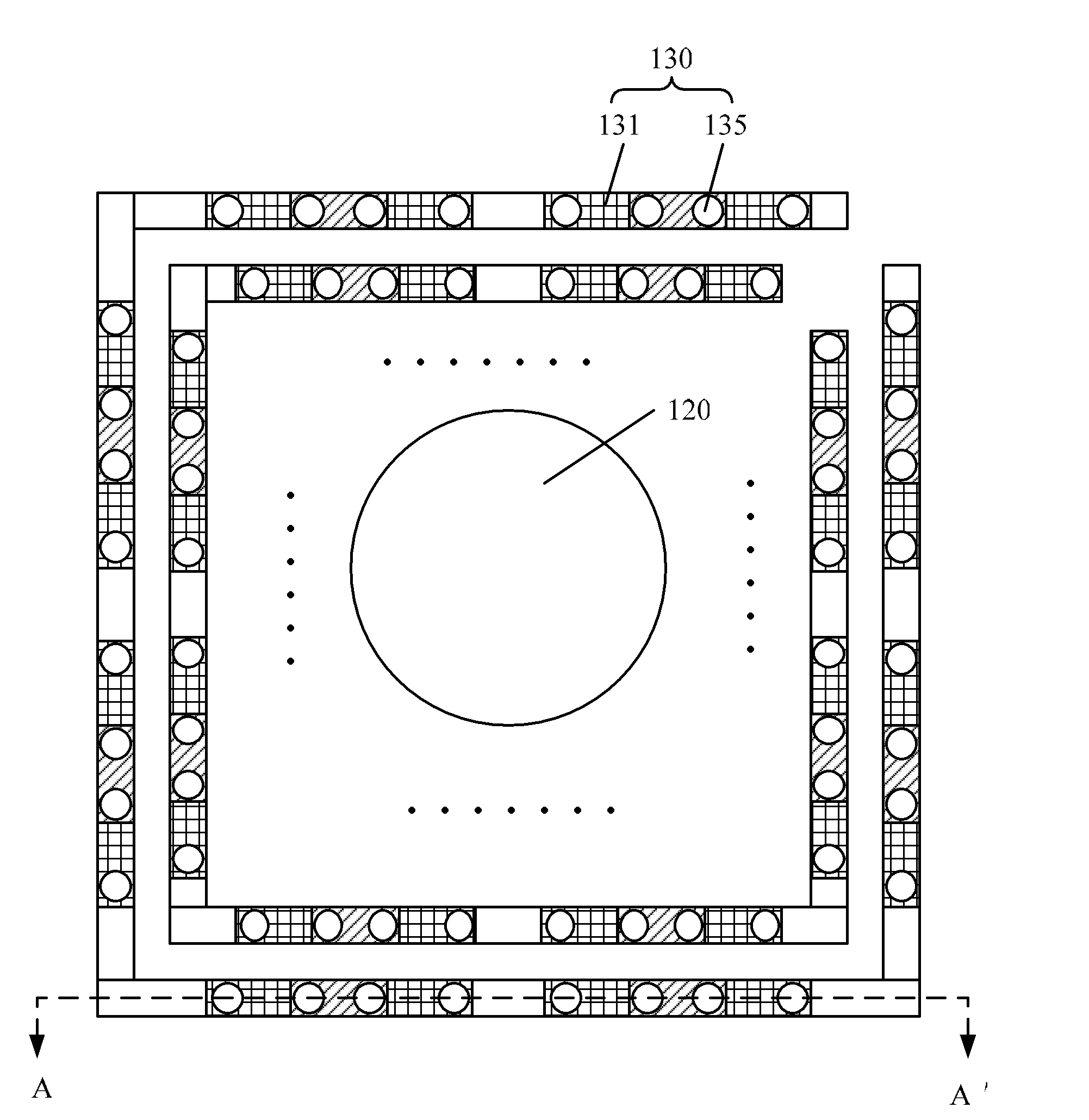
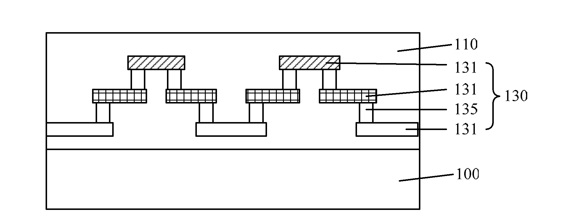
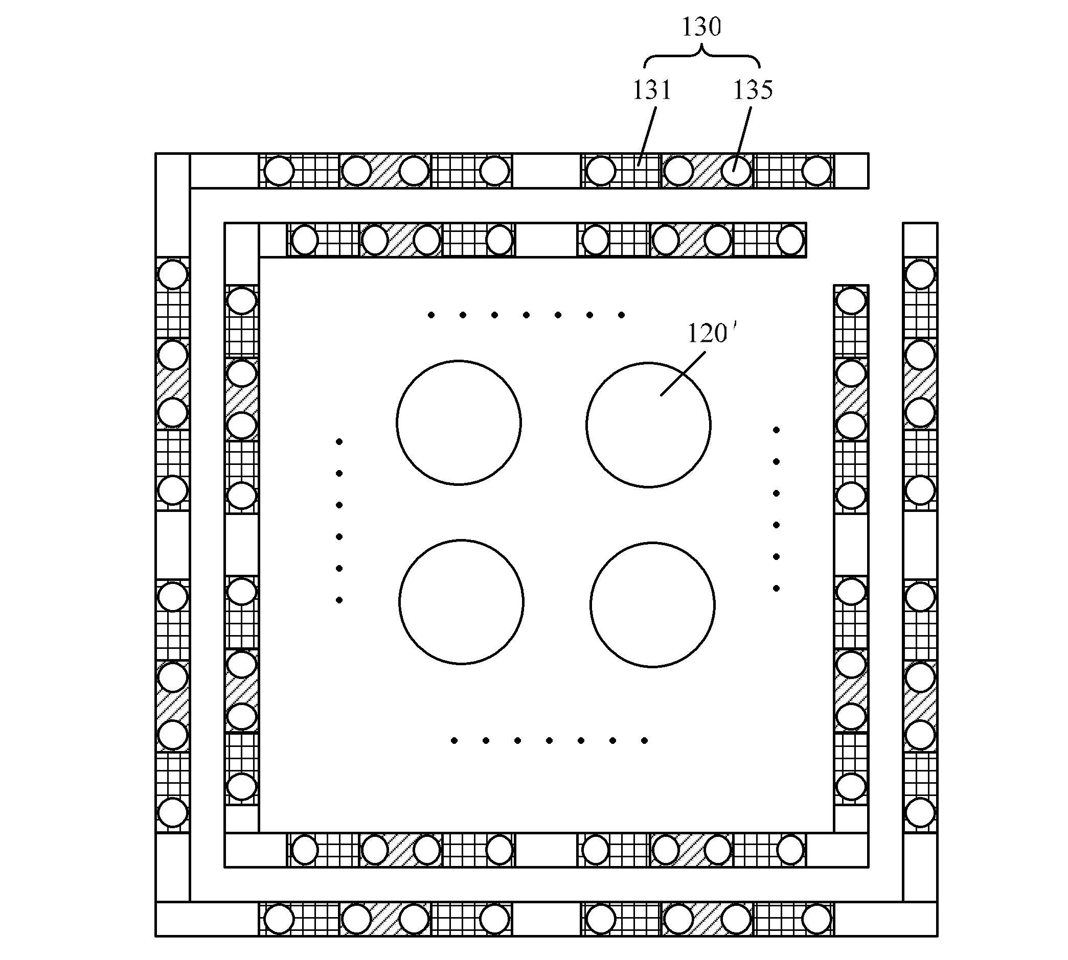
[0034] In the prior art, in order to realize three-dimensional stacking of chips, through-silicon vias penetrate the entire semiconductor substrate to realize electrical connection between the upper and lower chips. Wherein, the TSV is filled with copper. However, when the temperature of the semiconductor substrate changes, due to the thermal expansion coefficient mismatch between the copper and the semiconductor substrate, it is easy to cause the TSV to generate tensile or compressive stress on the surrounding semiconductor substrate and interlayer dielectric layer, The tensile or compressive stress changes the lattice of the interlayer dielectric layer and the metal interconnection layer finally formed around the TSV, thereby changing the electrical properties of the interconnection structure. Moreover, as more and more integrated circuits use low-K dielectric materials as the material of the interlayer dielectric layer, due to the low mechanical strength of the low-K dielec...


PUM


Abstract

The invention discloses a through-silicon via (TSV) testing structure and a TSV testing method. The TSV testing structure comprises a semiconductor substrate, an interlayer dielectric layer located on the surface of the semiconductor substrate, a TSV formed in the semiconductor substrate and the interlayer dielectric layer, and at least one interconnection structural ring, wherein the interconnection structural ring is distributed in an annular shape on the periphery of the TSV regarding the TSV as the center and is formed by metal layers on different layers, and electric conduction plugs between the metal layers in a serial-connection mode. Due to the fact that the interconnection structural ring is distributed in the annular shape on the periphery of the TSV regarding the TSV as the center, resistance of the interconnection structural ring is tested in directions far away from the TSV in sequence, tested resistance values are compared with a reference resistance value, then the range of an isolation region between the interconnection structural ring and the TSV can be obtained, and therefore the TSV testing structure and the TSV testing method are convenient and fast to use.

Description

technical field [0001] The invention relates to the technical field of semiconductor testing, in particular to a through-silicon via testing structure and a testing method for testing the range in which the stress of the through-silicon via has an influence on the interconnection structure. Background technique [0002] With the rapid development of portable electronic devices such as mobile phones, the size of portable electronic devices has become smaller and smaller, and the functions provided have become more and more extensive. Therefore, it is very necessary to improve the built-in chip without increasing the size of the device. level of integration. At present, three-dimensional packaging has become a method that can effectively improve chip integration. Current three-dimensional packaging includes die stacking based on gold wire bonding, package stacking and three-dimensional stacking based on through silicon vias (Through Silicon Via, TSV). Among them, the three-d...

Claims


Application Information

Patent Timeline
Patent Type & Authority Applications(China)
IPC IPC(8): H01L23/544G01R31/26G01B7/32
Inventor 冯军宏甘正浩
Owner SEMICON MFG INT (SHANGHAI) CORP
Why Eureka
Try Eureka