Conductive adhesive composition, electronic device, positive electrode laminate, and method for manufacturing electronic device

A conductive adhesive and electronic device technology, applied in the direction of conductive adhesives, semiconductor/solid device manufacturing, conductors, etc., can solve the problems of reduced carrier injection efficiency, low interface adhesion, and low conductivity of the bonding layer , to achieve excellent adhesion, low surface resistance and high transparency

Active Publication Date: 2013-07-03
LINTEC CORP
View PDF7 Cites 16 Cited by
  • Summary
  • Abstract
  • Description
  • Claims
  • Application Information

AI Technical Summary

Problems solved by technology

[0007] However, its use is limited in applications where cleanliness and uniformity of the interface are important factors through the lamination process of an adhesive layer containing a conductive organic polymer compound.
In addition, there are problems such as low conductivity of the adhesive layer, low carrier injection efficiency at the lamination interface, or low adhesion of the interface, etc., which lowers the performance of the electronic device.

Method used


Image

  • Conductive adhesive composition, electronic device, positive electrode laminate, and method for manufacturing electronic device
  • Conductive adhesive composition, electronic device, positive electrode laminate, and method for manufacturing electronic device
  • Conductive adhesive composition, electronic device, positive electrode laminate, and method for manufacturing electronic device

Examples


preparation example Construction

[0137] (4) Preparation method of electronic device

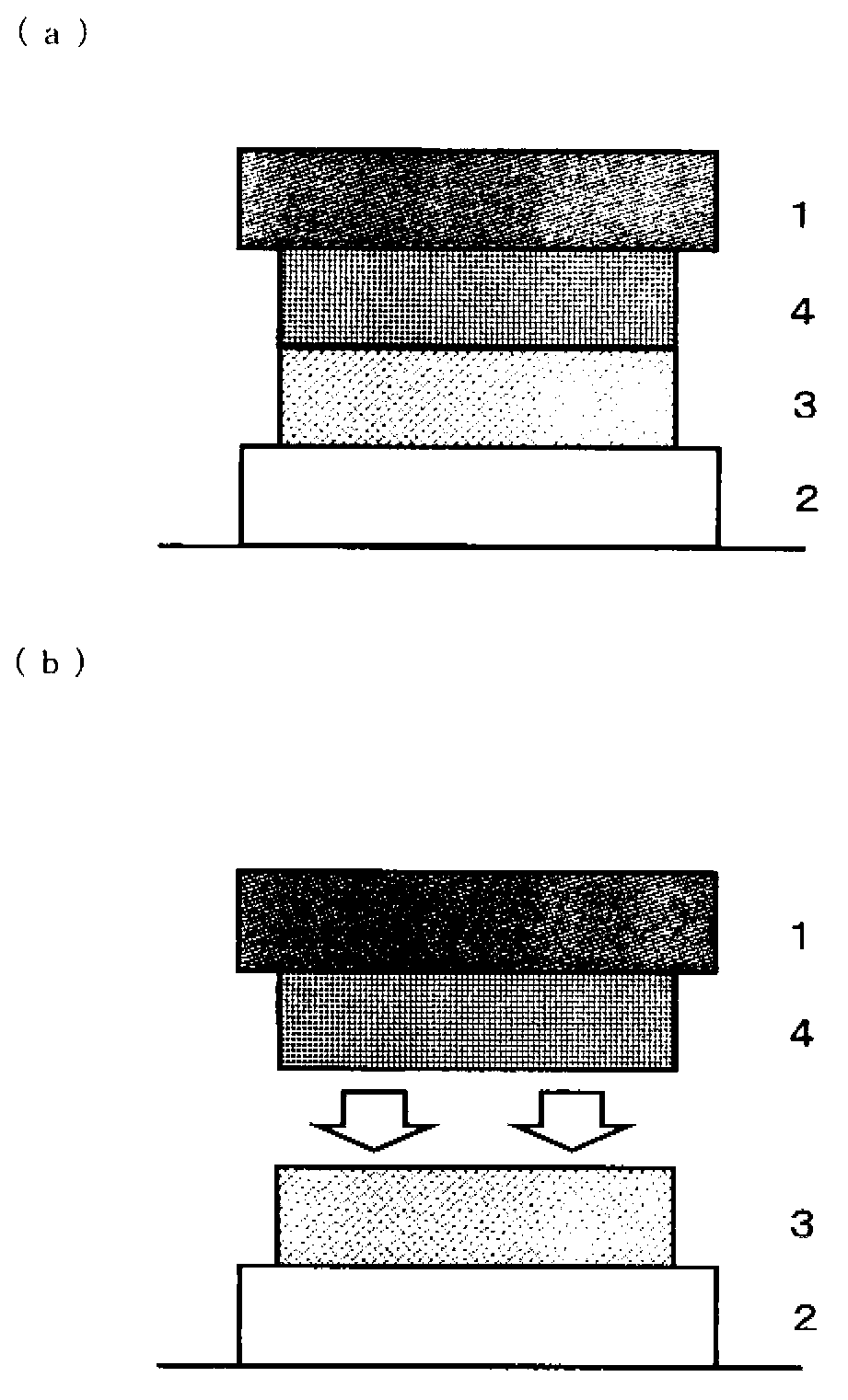
[0138] The manufacturing method of the electronic device of the present invention is characterized in that the step of forming a conductive layer formed of the conductive adhesive composition on the anode layer to form an anode laminate; forming the step of forming the anode layer on the cathode layer A step of forming a photoelectric conversion layer or a light-emitting layer to form a cathode laminate; above the temperature at which the conductive adhesive composition softens, the surface of the photoelectric conversion layer or light-emitting layer of the cathode laminate is bonded to the anode layer The conductive layer surface of the pressing body is bonded.

[0139] Below, through figure 1 (b) The method of manufacturing the electronic device of the present invention will be described in order.

[0140] The integration of the anode layer 1 and the conductive layer 4 is referred to as an anode laminate (described late...

Embodiment 1

[0158] [Preparation of conductive adhesive composition]

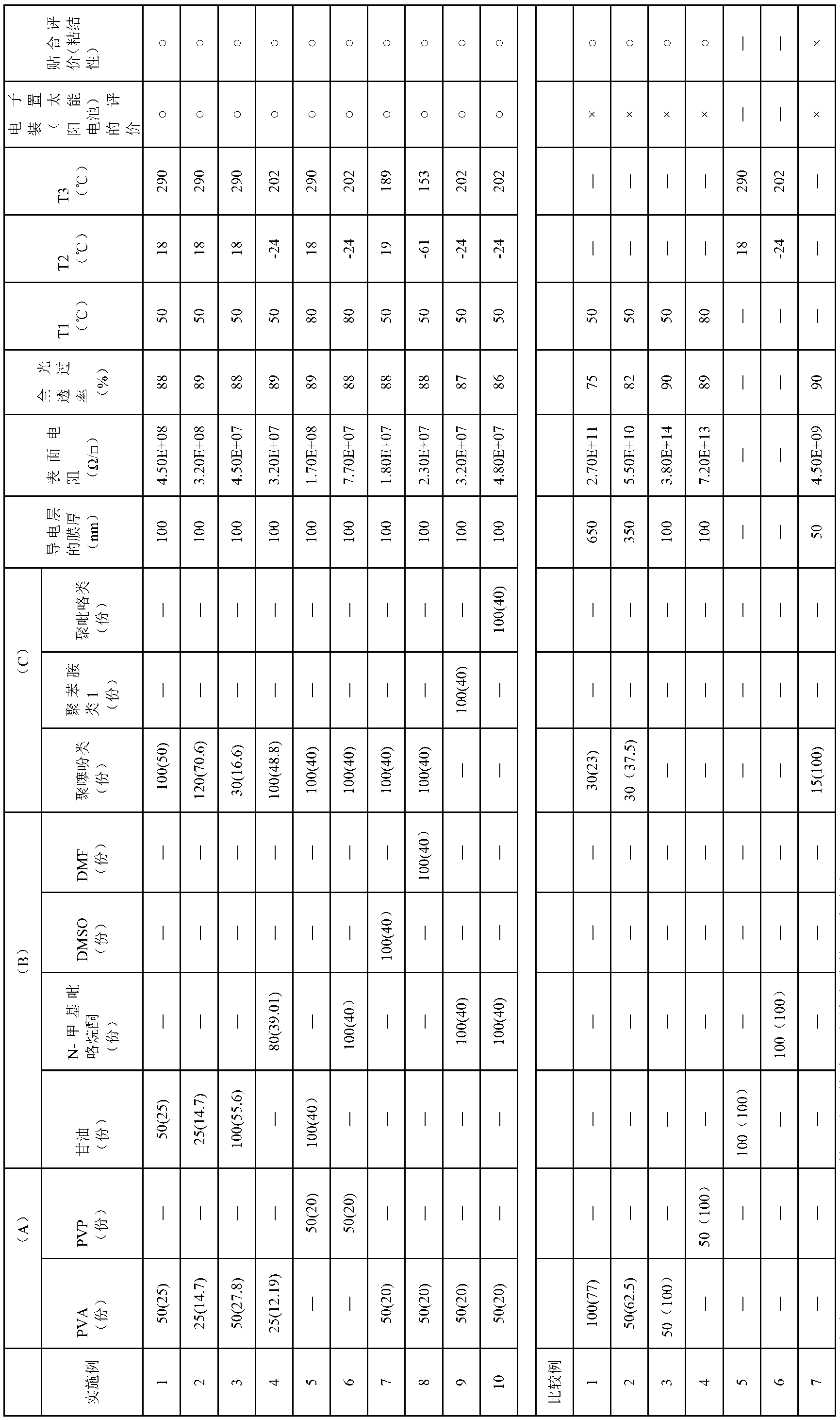
[0159] As the water-soluble polyvinyl polymer of component (A), 50 parts by mass of polyvinyl alcohol [manufactured by Sigma Aldrich Co., Ltd., product name "polyvinyl alcohol", molecular weight Mw = 9100, Tg (T1): 50°C, It is recorded as PVA in Table 1]. As the organic additive of the component (B), 50 parts by mass of glycerin [manufactured by Sigmardrich Co., Ltd., product name "glycerin", melting point (T2): 18° C., boiling point (T3): 290° C.] was used. As the conductive polymer polythiophenes of the component (C), 10,000 parts by mass of a mixture of poly(3,4-ethylene oxidethiophene) (PEDOT) and polystyrene sulfonic acid (PSS) (PEDOT:PSS ) [manufactured by H.C. Starck, product name "Clevious PVP.AI4083, active ingredient 1% by mass", described as polythiophenes in Table 1].

[0160] The components (A), (B) and (C) were dissolved in 200 parts by mass of pure water to prepare a coating solution of a conductive adh...

Embodiment 2、3

[0170] Except having changed to the blending of the following Table 1, it carried out similarly to Example 1, and obtained the electronic device.


PUM

PropertyMeasurementUnit
boiling pointaaaaaaaaaa
melting pointaaaaaaaaaa

Abstract

The present invention provides a conductive adhesive composition that has superior adhesive properties and low surface resistance and is capable of use as a buffer layer foran electronic device. This conductive adhesive composition contains a water-soluble polyvinyl polymer (A), organic additive (B), and conductive high molecular weight organic compound (C). The organic additive (B) is at least one selected from water-soluble polyhydric alcohols, water-soluble pyrrolidones, or hydrophilic aprotic solvents. The conductive high molecular weight organic compound (C) is at least one selected from polyanilines, polypyrroles, or polythiophenes as well as derivatives thereof. Furthermore, the present invention provides an electronic device having a conductive layer formed from this conductive adhesive composition, a positive electrode laminate in which a conductive layer formed from this conductive adhesive composition is laminated, and a method for manufacturing this electronic device.

Description

technical field [0001] The present invention relates to a conductive adhesive composition, an electronic device, an anode laminate, and a method for preparing the electronic device. Background technique [0002] In recent years, transparent electrodes using transparent conductive films have been actively studied in organic electroluminescence, various solar cells, touch panels, mobile phones, and electronic paper. [0003] For example, organic photoelectric conversion or electro-optical conversion devices typified by organic thin-film solar cells are generally produced by laminating materials on electrodes composed of transparent conductive films. As transparent conductive films, various conductive films such as metal thin films, metal oxide thin films, and conductive nitride thin films are being studied. Since they can have both light transmittance and electrical conductivity and excellent durability, metal oxide films are mainly used at present. Thin film is the mainstrea...

Claims


Application Information

Patent Timeline
Patent Type & Authority Applications(China)
IPC IPC(8): C09J157/00C09J9/02C09J11/00C09J129/04C09J139/06C09J179/00H01B1/12H01L51/42
CPCC09J139/06C09J179/02H01B1/127H01B1/128C09J165/00C08G2261/3221C08G2261/3223C08K5/053C08K5/3415C09J9/02C09J11/06C09J11/08C09J133/04C08L2203/204C09D165/00C09J125/18C09J129/04C08K5/20C08K5/41C08L29/04C08L33/02C08L39/06C08L65/00C08L79/00C08L81/00C08L2205/03Y10T428/2804Y02E10/549Y02P70/50H10K71/50H10K50/15C09J157/00C09J11/00H01B1/12H10K30/81H10K50/805
Inventor 加藤邦久武藤豪志中岛惠美
Owner LINTEC CORP
Why Eureka
Try Eureka