Vertical coupling grating coupler bonded by metal and manufacturing method thereof

A grating coupler and vertical coupling technology, which is applied in the coupling of optical waveguides and other directions, can solve the problems of reduced coupling efficiency in the vertical direction and increased difficulty in device packaging.

Active Publication Date: 2013-07-10
BEIJING UNIV OF TECH
View PDF5 Cites 32 Cited by
  • Summary
  • Abstract
  • Description
  • Claims
  • Application Information

AI Technical Summary

Problems solved by technology

However, for the traditional grating structure, due to the limitation of its symmetry on the single-side coupling efficiency, it is necessary to tilt the optical fiber at an angle of about 10° for incident and reception, which increases the difficulty of device packaging and alignment. Coupling scheme for direct vertical coupling
[0004] The vertically coupled grating coupler can use the negative first-order diffraction effect of the grating to achieve vertical coupling, but at the same time, due to the negative second-order reflection, diffraction to the substrate and transmission through the grating, the coupling efficiency in the vertical direction is reduced.

Method used


Image

  • Vertical coupling grating coupler bonded by metal and manufacturing method thereof
  • Vertical coupling grating coupler bonded by metal and manufacturing method thereof
  • Vertical coupling grating coupler bonded by metal and manufacturing method thereof

Examples


Embodiment Construction

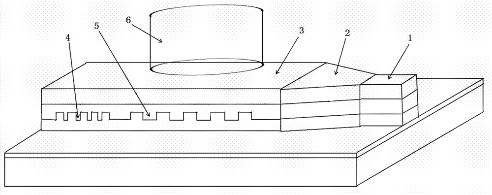
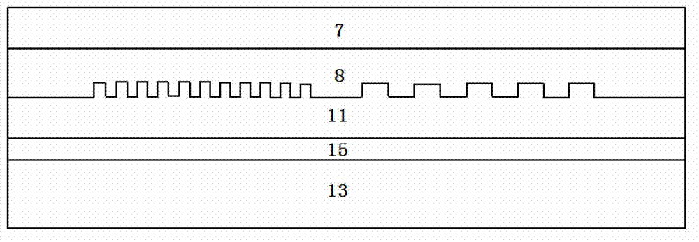
[0054] The structure and features of the present invention will be further described in detail below in conjunction with the drawings and embodiments. Such as figure 1 , figure 2 As shown, a metal-bonded vertical coupling grating coupler, including:

[0055] A carrier sheet 13, which is a silicon sheet or a glass sheet;

[0056] A reflective mirror layer 15 doubles as a bonding layer, and the reflective mirror layer is made of gold material; the thickness of the reflector is not less than 50nm; it can highly reflect the vertically downward diffracted light of the coupling grating, so as to improve the distance between the silicon waveguide core layer 8 and the optical fiber 6. Coupling efficiency between;

[0057] A lower confinement layer 11, the lower confinement layer 11 is a DVS-BCB material;

[0058] A silicon waveguide core layer 8, the waveguide core layer 8 is fabricated under the upper confinement layer 7; the thickness of the waveguide core layer 8 is not greate...


PUM


Abstract

The invention relates to the technical field of photonic devices, in particular to a vertical coupling grating coupler bonded by metal and a manufacturing method thereof. The grating coupler comprises a carrier piece, a metal bonding layer serving as a reflective mirror layer, a lower limiting layer of slab waveguide, tapered waveguide and submicron waveguide, a sandwich layer of the slab waveguide, the tapered waveguide and the submicron waveguide , an upper limiting layer of the slab waveguide, the tapered waveguide and the submicron waveguide and an optical fiber, wherein the carrier piece is formed by a silicon wafer or a glass sheet, the lower limiting layer is formed by a DVS-BCB layer, the sandwich layer is formed by a silicon layer, the upper limiting layer is formed by a silicon oxide oxidation layer, the slab waveguide, the tapered waveguide and the submicron waveguide are mutually linked up in the horizontal direction, a coupling grating and a reflecting grating are manufactured on the surface of the slab waveguide sandwich layer, and one end of the optical fiber is vertically close to the surface of the upper limiting layer of an SOI with a silicon substrate removed. According to the vertical coupling grating coupler, high-efficiency vertical coupling between the optical fiber and planar optical waveguide can be realized.

Description

technical field [0001] The invention relates to the fields of optical communication and optical interconnection, in particular to the design and preparation of a coupling structure of an optical waveguide. The structure of the grating coupler can effectively reduce the coupling loss when the optical fiber and the waveguide are vertically coupled. Background technique [0002] With the development of micro-nano optoelectronic technology, the size of optoelectronic devices is getting smaller and smaller. Especially in silicon-based photonics, the optical waveguide material selected is silicon, and the SOI structure is adopted. Due to the large refractive index difference of the SOI optical waveguide device, it has the advantages of small device size and high integration, but at the same time its small size The small device size also brings coupling and alignment difficulties to silicon-based integrated optical systems. The cross-sectional size of the SOI waveguide is hundred...

Claims


Application Information

Patent Timeline
Patent Type & Authority Applications(China)
IPC IPC(8): G02B6/34
Inventor 郭霞武华韩明夫
Owner BEIJING UNIV OF TECH
Why Eureka
Try Eureka