Method for machining concave reflection surface on side surface of optical waveguide based on laser stepped etching method

A technology of side processing and step reflection, which is applied in the coupling of optical waveguide, optical waveguide light guide, light guide, etc., can solve the problems of numerical aperture mismatch and low coupling efficiency, achieve high processing accuracy, improve coupling efficiency, and benefit the optical back The effect of board space integration

Inactive Publication Date: 2017-08-11
SHANGHAI UNIV
View PDF7 Cites 3 Cited by
  • Summary
  • Abstract
  • Description
  • Claims
  • Application Information

AI Technical Summary

Problems solved by technology

[0005] The invention intends to solve the problem of low coupling efficiency due to the mismatch of numerical aperture when the optical waveguide-fiber is vertically coupled, and proposes a method for processing a concave reflective surface on the side of the optical waveguide based on the laser step etching method

Method used


Image

  • Method for machining concave reflection surface on side surface of optical waveguide based on laser stepped etching method
  • Method for machining concave reflection surface on side surface of optical waveguide based on laser stepped etching method
  • Method for machining concave reflection surface on side surface of optical waveguide based on laser stepped etching method

Examples


Embodiment 1

[0026] join Figure 8 , this embodiment proposes a processing flow for processing a concave reflective surface on the side of an optical waveguide based on a laser step etching method.

[0027] Firstly, determine a number of continuous sub-processing areas whose axes are in a straight line on the side of the optical waveguide, and these sub-processing areas form a total processing area; then, according to the specific concave shape etched (such as parabola, double Curve, arc, free curve), determine the maximum depth of each sub-processing area, in order to determine the number of steps, step width, and step depth to be processed in each sub-processing area; then, process each sub-processing area separately, specifically When etching, each sub-processing area determines at least two or partially overlapping areas, and the etching depth of the overlapping area is twice the etching depth of the non-overlapping area of ​​the previous etching, thus forming a regular stepped reflect...

Embodiment 2

[0029] join Figure 1-Figure 9 , the present embodiment is basically the same as Embodiment 1, and its special features are as follows:

[0030] First, when the total processing area is guaranteed to be constant, the more the number of sub-processing areas is determined, the closer the processed stepped reflective concave surface is to the designed concave surface shape, and the better the reflective focusing effect will be.

[0031] Second, when selecting processing parameters, two processing methods can be selected to process the concave shape to be designed. One method is: control the number of steps to decrease in sequence, the step width to decrease in sequence, but the step depth is the same, and the other method It is: the number of control steps is the same, the step width is the same, but the step depth decreases successively.

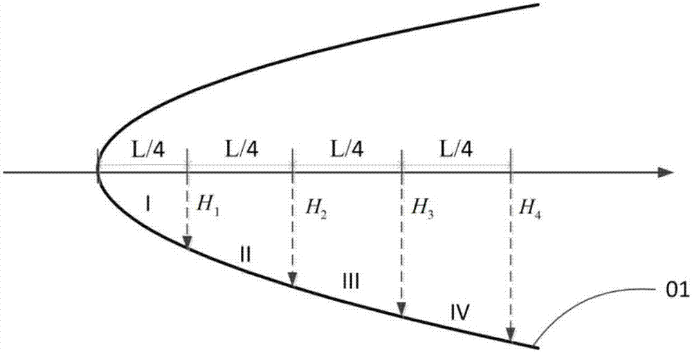
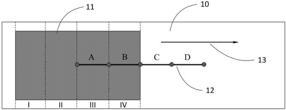
[0032] The third is to describe the specific etching process by determining 4 sub-processing areas with equal lengths. The total length of t...

Embodiment 3

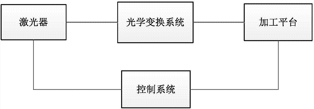
[0036] This embodiment provides a more specific method for processing a concave reflective surface on the side of an optical waveguide based on the laser step etching method. parameter optional, figure 1 A schematic diagram of the equipment system for concave machining is shown.

[0037] In this embodiment, a kind of similar etching is determined on the optical waveguide figure 2 As shown in the parabolic reflective surface 01, the parabolic reflective surface reflects the parallel beam parallel to the parabolic axis and converges the reflected beam to its focal point. The focal point position can be determined according to the actual requirements of the fiber-optical waveguide vertical coupling. When the focal point position After selection, the etched parabola is uniquely determined. figure 2 The example is divided into 4 equally spaced areas I, II, III, and IV on the parabola 010, and the maximum depth of each area is H 1 、H 2 、H 3 、H 4 . In the optical waveguide 1...


PUM


Abstract

The invention proposes a method for machining a concave reflection surface on a side surface of an optical waveguide based on a laser stepped etching method. The method comprises the machining steps: determining a plurality of continuous machining subareas on a side surface of the optical waveguide, wherein the axial directions of the machining subareas are located one the same line, and the machining subareas form a total machining area; determining the machining depth, the number of steps, the step width and the step depth of each area according to the specific shape of the concave surface; carrying out the machining of each machining subarea, determining at least two areas or a part of overlapped area of each machining subarea, and carrying out the etching so as to form a regular stepped reflection surface. The numbers of steps, step widths and step depths of all machining subareas need to be set specifically, and can be the same and also can be different. However, the subareas have different maximum depths and the stepped reflection concave surfaces corresponding to the maximum depths of the concave surfaces in a one-to-one manner. The stepped reflection concave surfaces can serve as concave surface reflectors of the optical waveguide. The prepared two-side stepped reflection concave surfaces are processed through a postprocessing method or a machining process laser shading method, thereby obtaining single-side stepped reflection concave surfaces. The method provided by the invention is simple in flow, is high in machining precision, and can achieve the batch production.

Description

technical field [0001] The invention relates to the field of micromachining and manufacturing, and proposes a method for processing a concave reflection surface on the side of an optical waveguide based on a laser step etching method. Background technique [0002] With the rapid development of broadband communications, supercomputers and big data centers, the traditional Printed Circuit Board (PCB) interconnection technology has revealed a bottleneck in high-speed bandwidth (50Gbps) processing capabilities, while PCB-based optical interconnections Backplane technology has developed rapidly due to its many advantages such as high bandwidth, low energy consumption, no electromagnetic interference, and low cost. It is expected to become the mainstream interconnection method between daughterboards and backplanes, backplanes, and modules in the future. [0003] In the application of optical interconnection backplane technology, how to realize the efficient coupling between optica...

Claims


Application Information

Patent Timeline
IPC IPC(8): G02B6/13G02B6/122G02B6/12G02B6/26
CPCG02B6/13G02B6/12G02B6/122G02B6/26G02B2006/12104
Inventor 王廷云邓传鲁陈佳敏庞拂飞严新捷
Owner SHANGHAI UNIV
Why Eureka
Try Eureka