Cladding material for insulated substrates

A technology of insulating substrates and cladding materials, which is applied in the directions of welding/cutting media/materials, applications, household appliances, etc., and can solve problems such as the inability to install semiconductor components

Inactive Publication Date: 2013-07-17
SHOWA DENKO KK
View PDF11 Cites 6 Cited by
  • Summary
  • Abstract
  • Description
  • Claims
  • Application Information

AI Technical Summary

Problems solved by technology

[0006] Here, when the Ni layer such as the Ni plating layer formed on the metal layer of the insulating substrate has a thickness of about several μm, due to the heat applied when the insulating substrate and the heat dissipation member are joined by brazing, and / Or the heat applied when joining the semiconductor element to the insulating substrate by soldering may cause large unevenness on the surface of the Ni layer, and as a result, the mounting of the semiconductor element on the insulating substrate may not be substantially realized.

Method used


Image

  • Cladding material for insulated substrates
  • Cladding material for insulated substrates
  • Cladding material for insulated substrates

Examples


Embodiment 1

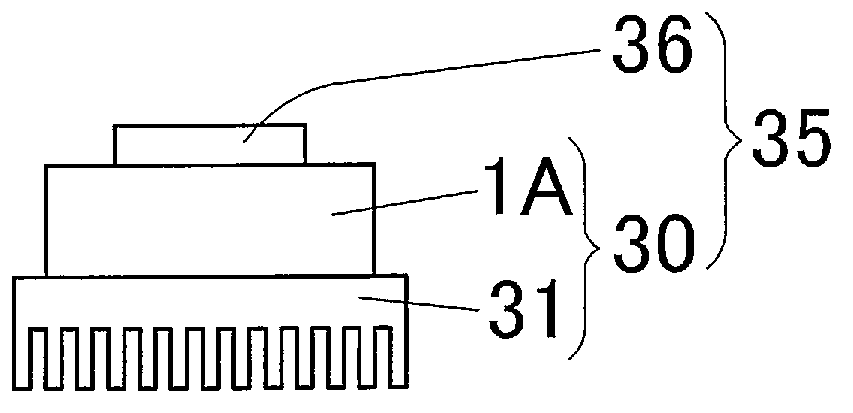
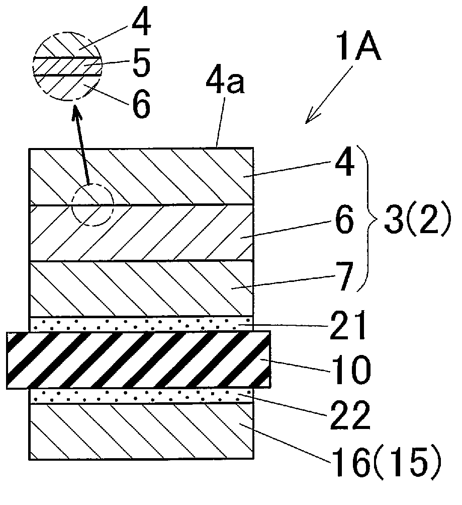
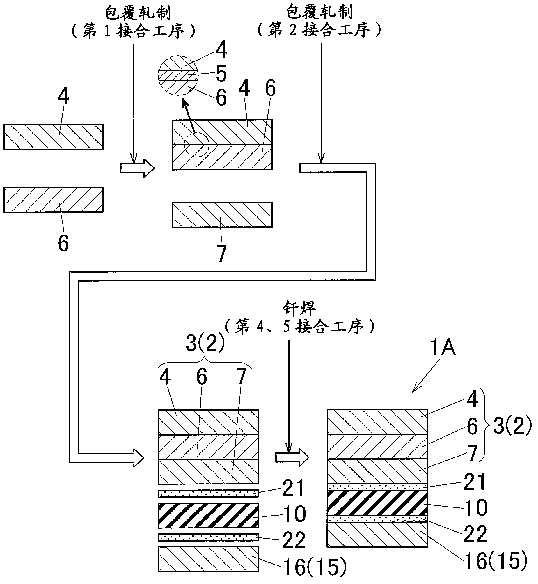
[0198] In this Example 1, a figure 2 and the insulating substrate 1A of the above-mentioned first embodiment shown in 3. Its production method is as follows.

[0199] The lower plate is prepared as the Ni layer 4, the Ti layer 6, the first Al layer 7, the ceramic layer 10, and the third Al layer 16, respectively.

[0200] Ni layer 4: a pure Ni plate with a length of 25 mm x a width of 25 mm x a thickness of 50 μm

[0201] Ti layer 6: a pure Ti plate with a length of 25 mm x a width of 25 mm x a thickness of 200 μm

[0202] The first Al layer 7: a pure Al plate with a length of 25 mm x a width of 25 mm x a thickness of 600 μm

[0203] Ceramic layer 10: AlN plate of 25 mm in length x 25 mm in width x 600 μm in thickness

[0204] The third Al layer 16: a pure Al plate with a length of 25 mm x a width of 25 mm x a thickness of 600 μm.

[0205] The purity of the Ni plate forming the Ni layer 4 is JIS (Japanese Industrial Standard) Class 1. The purity of the Ti plate forming ...

Embodiment 2

[0211] In this Example 2, a Figure 5 The insulating substrate 1B of the above-mentioned second embodiment is shown. Its production method is as follows.

[0212] Lower plates were prepared as Ni layer 4 , Ti layer 6 , first Al layer 7 , second Al layer 8 , ceramic layer 10 , and third Al layer 16 .

[0213] Ni layer 4: a pure Ni plate with a length of 25 mm x a width of 25 mm x a thickness of 20 μm

[0214] Ti layer 6: a pure Ti plate with a length of 25 mm x a width of 25 mm x a thickness of 20 μm

[0215] The first Al layer 7: a pure Al plate with a length of 25 mm x a width of 25 mm x a thickness of 40 μm

[0216] The second Al layer 8: a pure Al plate with a length of 25 mm x a width of 25 mm x a thickness of 600 μm

[0217] Ceramic layer 10: AlN plate of 25 mm in length x 25 mm in width x 600 μm in thickness

[0218] The third Al layer 16: a pure Al plate with a length of 25 mm x a width of 25 mm x a thickness of 600 μm.

[0219] The purity of the Ni plate forming ...

Embodiment 3

[0225] In this Example 3, the same method as in Example 2 above was produced Figure 5 The insulating substrate 1B of the above-mentioned second embodiment is shown. Its production method is as follows.

[0226] Lower plates were prepared as Ni layer 4 , Ti layer 6 , first Al layer 7 , second Al layer 8 , ceramic layer 10 , and third Al layer 16 .

[0227] Ni layer 4: a pure Ni plate with a length of 25 mm x a width of 25 mm x a thickness of 15 μm

[0228] Ti layer 6: a pure Ti plate with a length of 25 mm x a width of 25 mm x a thickness of 15 μm

[0229] The first Al layer 7: an Al plate with a length of 25 mm x a width of 25 mm x a thickness of 100 μm

[0230] The second Al layer 8: a pure Al plate with a length of 25 mm x a width of 25 mm x a thickness of 600 μm

[0231] Ceramic layer 10: AlN plate of 25 mm in length x 25 mm in width x 600 μm in thickness

[0232] The third Al layer 16: a pure Al plate with a length of 25 mm x a width of 25 mm x a thickness of 600 μm....


PUM

PropertyMeasurementUnit
thicknessaaaaaaaaaa
thicknessaaaaaaaaaa
thicknessaaaaaaaaaa

Abstract

A cladding material (1A) is provided with: a Ni layer (4) made from Ni or a Ni alloy; a Ti layer (6) formed from Ti or a Ti alloy and positioned on one side of the Ni layer (4); and a first Al layer (7) formed from Al or Al alloy and positioned on the other side of the Ti layer (6) to which the Ni layer (4) is positioned. The Ni layer (4) and Ti layer (6) are joined by cladding rolling. A Ni-Ti superelastic layer (5) formed by alloying at least the Ni of the constituent elements of the Ni layer (3) and at least the Ti of the constituent elements of the Ti layer (6) is interposed between the Ni layer (4) and the Ti layer (6). The Ti layer (6) and the first Al layer (7) adjoin one another and are joined by cladding rolling.

Description

technical field [0001] The present invention relates to a covering material for an insulating substrate used for heat dissipation of a semiconductor element, a manufacturing method thereof, a base (base) for a semiconductor module, and a semiconductor module. [0002] In addition, in this specification, the term "board" is used in the meaning including "foil". Background technique [0003] Semiconductor modules such as power semiconductor modules dissipate heat generated from semiconductor elements due to the operation of the semiconductor elements, and therefore include heat dissipation components (eg, heat sinks, coolers). Furthermore, in this semiconductor module, a heat dissipation insulating substrate for transferring heat generated from the semiconductor element to the heat dissipation member is arranged between the semiconductor element and the heat dissipation member. Although this insulating substrate is a thermal conductor, it functions as an electrical insulator....

Claims


Application Information

Patent Timeline
Patent Type & Authority Applications(China)
IPC IPC(8): H01L23/14B32B15/01B32B15/04
CPCB23K1/0016H01L23/3735B32B15/017B32B15/01B23K2201/40B23K35/0222B23K35/0238B23K35/286B23K35/325B32B9/005B32B9/041B32B15/20B32B2307/206B32B2307/302B32B2307/51B32B2307/734B32B2457/00B32B2457/14B23K2101/40C22C14/00C22C19/03C22C21/00H01L2924/0002Y10T156/10Y10T428/12611Y10T428/12743H01L2924/00B32B15/04H01L23/14
Inventor 大泷笃史大山茂
Owner SHOWA DENKO KK
Why Eureka
Try Eureka