Printed circuit board silk screen hole plugging method

A technology of printed circuit boards and printed circuits, applied in the direction of electrical connection formation of printed components, etc., can solve problems such as low efficiency, high production cost, and easy occurrence of foaming and cavitation

Active Publication Date: 2013-07-24
MEIZHOU ZHIHAO ELECTRONICS TECH
View PDF5 Cites 13 Cited by
  • Summary
  • Abstract
  • Description
  • Claims
  • Application Information

AI Technical Summary

Problems solved by technology

[0004] In the prior art, the solder resist plug holes for via holes are usually made by aluminum sheet plug hole technology, which is prone to foaming and cavitation, and the production cost is high and the efficiency is low, which is difficult to meet the demand

Method used


Image

  • Printed circuit board silk screen hole plugging method
  • Printed circuit board silk screen hole plugging method
  • Printed circuit board silk screen hole plugging method

Examples


Embodiment Construction

[0021] The following will clearly and completely describe the technical solutions in the embodiments of the present invention. Obviously, the described embodiments are only some of the embodiments of the present invention, rather than all the embodiments. Based on the embodiments of the present invention, all other embodiments obtained by persons of ordinary skill in the art without making creative efforts belong to the protection scope of the present invention.

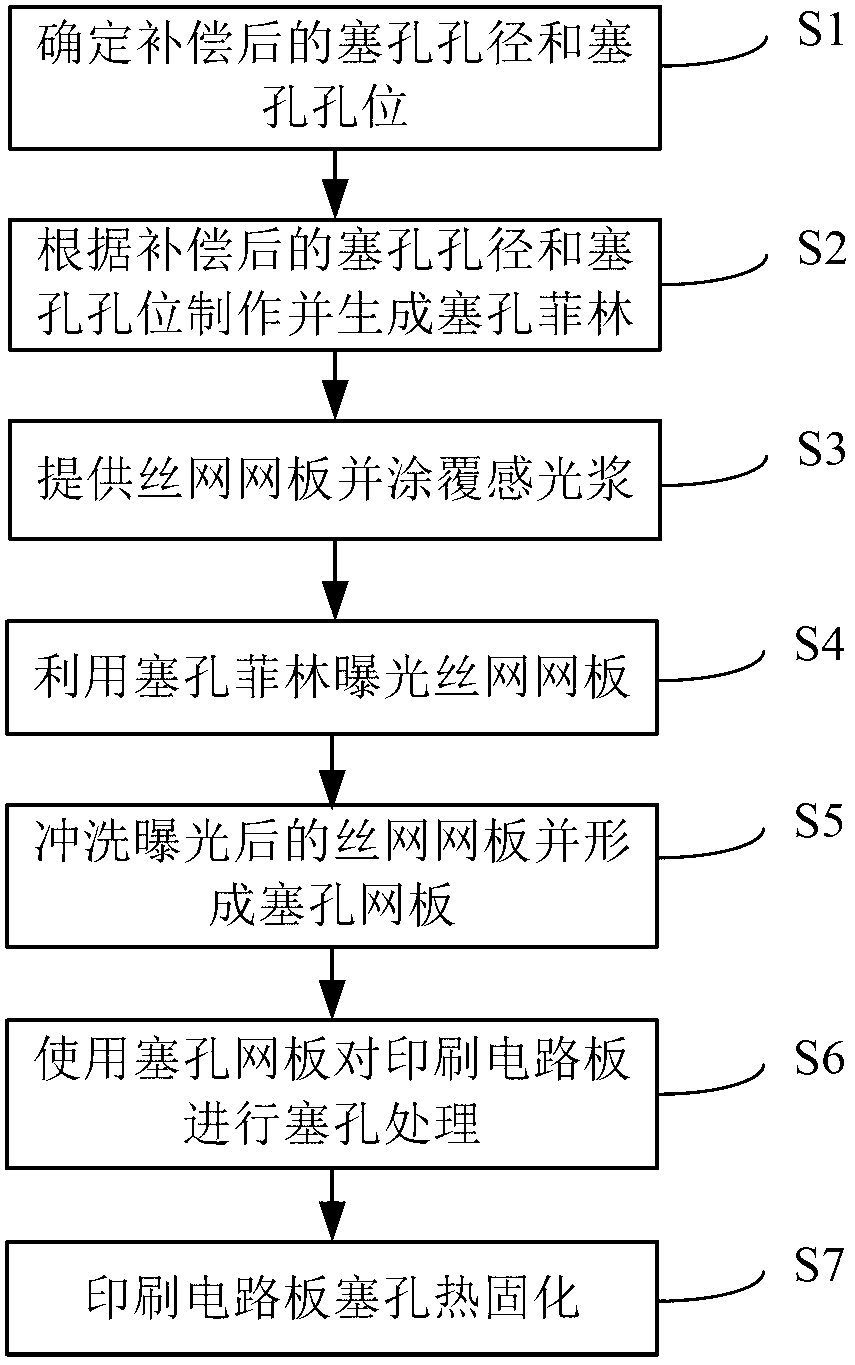
[0022] see figure 1 , is a flow diagram of a preferred embodiment of the printed circuit board screen plugging method of the present invention, and the embodiment includes:

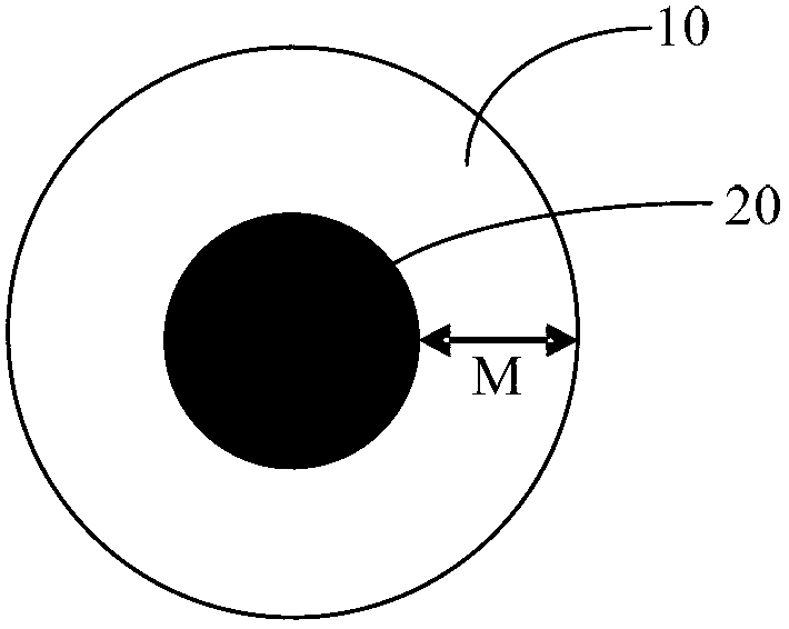
[0023] Step S1, determining the plug hole diameter and plug hole position after compensation. see figure 2 , is a schematic diagram of the hole diameter of the plug hole in this embodiment. like figure 2 As shown, the aperture diameter of a via hole 20 of the printed circuit board plus the compensation amount M to obtain the compensated pl...


PUM


Abstract

The invention provides a printed circuit board silk screen hole plugging method. The printed circuit board silk screen hole plugging method comprises the steps: the diameters and the positions of plug holes after compensation are determined; a plug hole film is manufactured and generated according to the diameters and the positions of the plug holes after the compensation; a silk screen board is provided and is coated with photosensitive paste; the silk screen board is exposed through the plug hole film; the silk screen board after exposure is developed and a plug hole screen board is formed; plug hole processing is conducted on a printed circuit board through the plug hole screen board; and thermofixation is conducted on the plug holes of the printed circuit board. The printed circuit board silk screen hole plugging method is capable of guaranteeing high generation efficiency, good product quality and low cost.

Description

technical field [0001] The invention relates to circuit board technology, in particular to a method for plugging holes with silk screen on a printed circuit (PCB, Printed Circuit Board) board. Background technique [0002] With the popularization and wide application of electronic products, the production and manufacturing technology of printed circuit boards are constantly updated and developed. In order to meet product requirements, PCB boards have been developed from single-layer boards to the design and application of double-layer boards or multi-layer boards, and there are via holes (Via Hole) between the multi-layer boards for inter-layer performance conduction. [0003] With the development of electronic products in the direction of "light, thin, short and small", the density of PCB is also getting higher and higher. In order to prevent short circuit and virtual soldering caused by tin penetrating from the via hole to the component surface during wave soldering, avo...

Claims


Application Information

Patent Timeline
Patent Type & Authority Applications(China)
IPC IPC(8): H05K3/40
Inventor 戴晖刘喜科林人道
Owner MEIZHOU ZHIHAO ELECTRONICS TECH
Why Eureka
Try Eureka