Liquid crystal display panel and manufacturing method thereof

A technology of liquid crystal display panels and substrates, which is applied in semiconductor/solid-state device manufacturing, optics, instruments, etc., and can solve problems such as large resistance and large voltage uniformity test

Active Publication Date: 2013-08-07
NANJING CEC PANDA LCD TECH
View PDF5 Cites 10 Cited by
  • Summary
  • Abstract
  • Description
  • Claims
  • Application Information

AI Technical Summary

Problems solved by technology

However, since the ITO layer in the pixel area has a double-layer structure, it is necessary to add a photomask, and the number of photomasks is large (6), and the common electrode formed by the ITO is limited by the pixel design, and it is necessary to use a contact hole

Method used


Image

  • Liquid crystal display panel and manufacturing method thereof
  • Liquid crystal display panel and manufacturing method thereof
  • Liquid crystal display panel and manufacturing method thereof

Examples


Embodiment Construction

[0039] Below in conjunction with the accompanying drawings and specific embodiments, the present invention will be further clarified. It should be understood that these embodiments are only used to illustrate the present invention and not to limit the scope of the present invention. Modifications of equivalent forms all fall within the scope defined by the appended claims of this application.

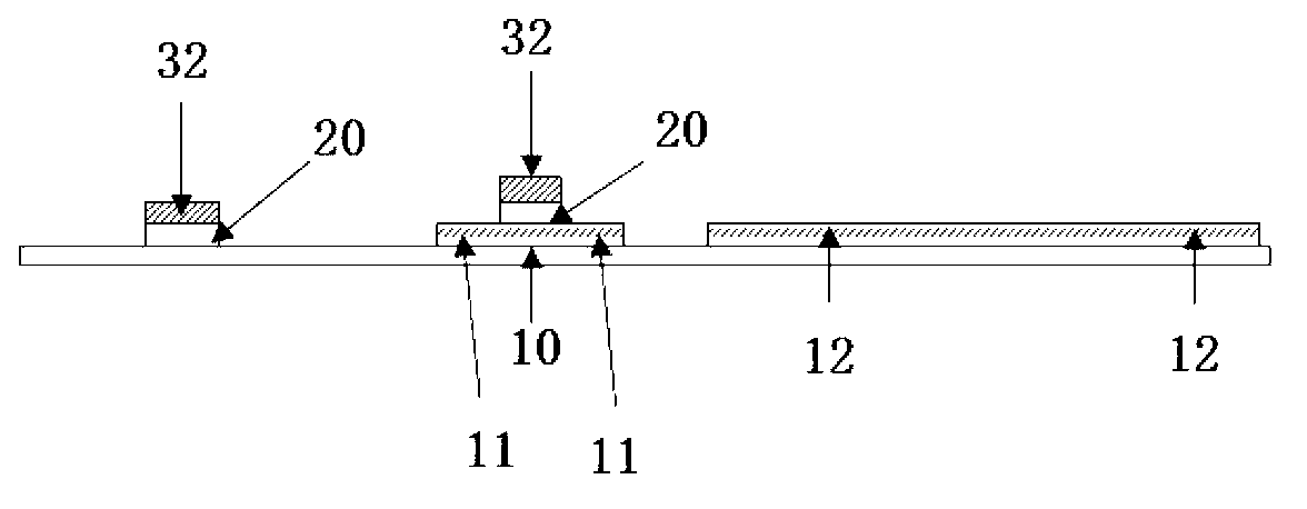
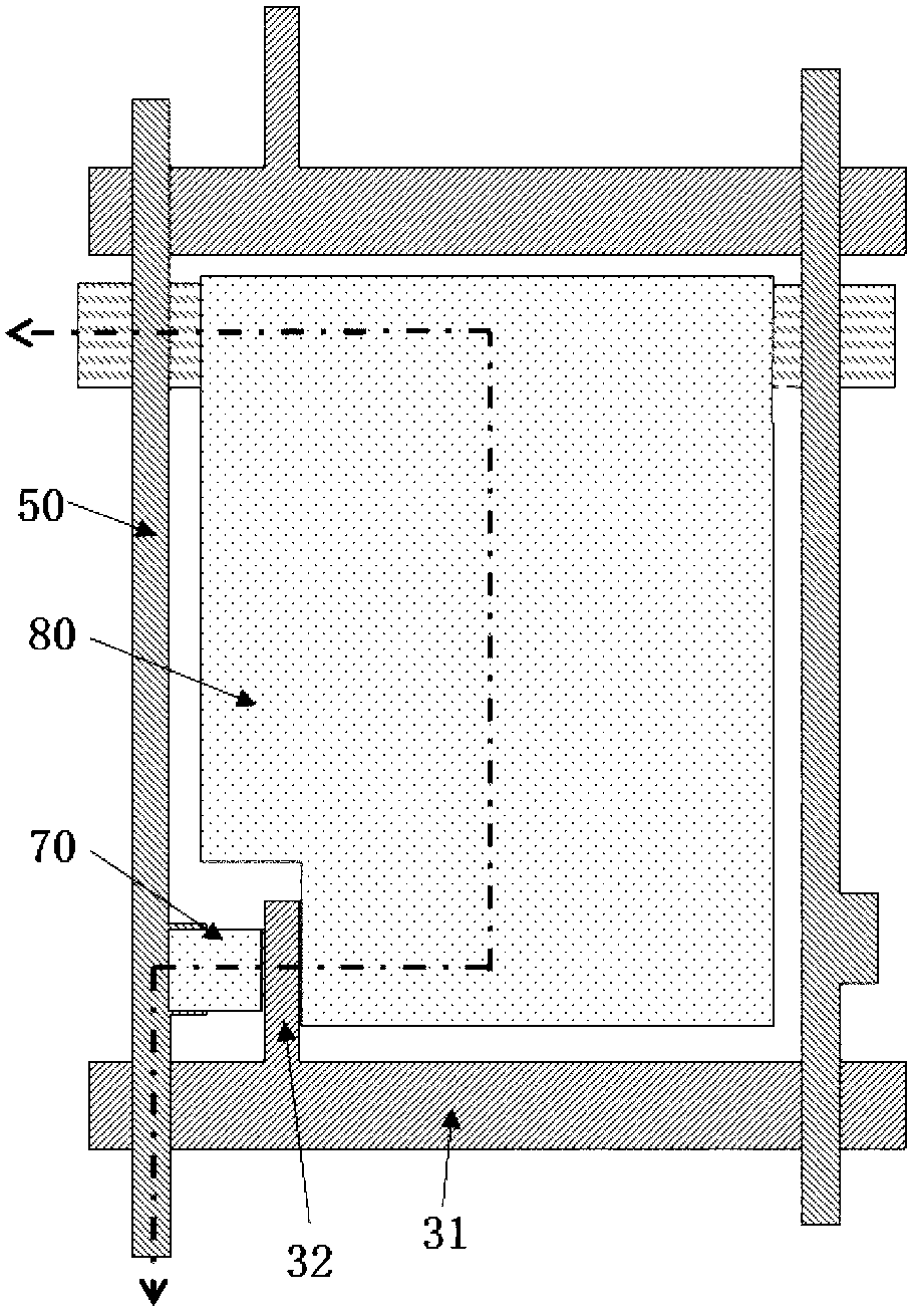
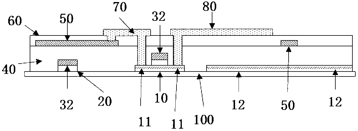
[0040] The present invention relates to a liquid crystal display panel, which comprises: data lines and scan lines crossed vertically and horizontally on a substrate, the data lines and scan lines intersect to define a pixel electrode, a thin film transistor, and a semiconductor layer in a pixel area, the thin film The transistor includes a gate electrode formed together with the scan line, a source electrode electrically connected to the data line, and a drain electrode electrically connected to the pixel electrode. The common electrode, the semiconductor layer, the transparent common ...


PUM


Abstract

The invention discloses a liquid crystal display panel and a manufacturing method thereof. The liquid crystal display panel comprises data lines, scanning lines and a semiconductor layer, wherein the data lines and the scanning lines are vertically and horizontally crossed on a substrate and used for crossly limiting pixel electrodes and thin film transistors in a pixel region; transparent public electrodes forming storage capacitors with the pixel electrodes are also arranged in the pixel region; each thin film transistor comprises a grid electrode, a source electrode and a drain electrode; the semiconductor layer is formed along with the transparent public electrodes; and the semiconductor layer and the transparent public electrodes are all positioned on the substrate. According to the liquid crystal display panel, few limitations are in the manufacturing process, so that the transparent public electrodes between adjacent pixels can be directly connected, the impedance of the transparent public electrodes is reduced, and the voltage distribution of the public electrodes is more uniform; and the manufacturing method is a mask-saving manufacturing process, so that the number of light masks in the manufacturing method of the liquid crystal panel with the transparent storage capacitors can be reduced to be 4 or 5, the production capacity can be increased, and the cost can be saved.

Description

technical field [0001] The present invention relates to a liquid crystal display panel and a manufacturing method thereof. Background technique [0002] The resolution of liquid crystal displays continues to improve, but the demand for environmental protection and energy saving also increases. In order to meet the aforementioned trend, the aperture ratio needs to be increased. Currently, there are designs using transparent electrodes as storage electrodes. [0003] BOE patent CN200910078374.4 proposes a TFT-LCD array substrate and its manufacturing method, which is to add a layer of ITO in the pixel area of ​​the array substrate and the pixel electrode ITO to form a storage capacitor. The storage capacitor will not affect the transmittance of the pixel area, thereby improving the aperture ratio and display brightness, and improving the display quality as a whole. In this way, although a larger storage capacitor can be formed, the kickback voltage and leakage can be reduced....

Claims


Application Information

Patent Timeline
IPC IPC(8): G02F1/1362G02F1/1368G02F1/1333H01L21/77
Inventor 吴剑龙
Owner NANJING CEC PANDA LCD TECH
Why Eureka
Try Eureka